
Method of manufacturing device having flexible substrate and device having flexible substrate manufactured using the same

Active Publication Date: 2007-05-10
LG DISPLAY CO LTD
View PDF12 Cites 73 Cited by
  • Summary
  • Abstract
  • Description
  • Claims
  • Application Information

AI Technical Summary

Benefits of technology

[0020] As described above, since the substrate that can be bent and is used to manufacture an organic light emitting device is formed on the mother substrate using the vacuum evaporation method, generation of dust, which is formed on the plastic substrate because of processes, such as injection, extrusion, and the like, is prevented. The roughness of the surface is also good enough to manufacture the organic light emitting device.
[0025] Preferably, a polymer used for the second polymer layer is the same as the polymer used for the first polymer layer because there is no stress due to difference in thermal expansion coefficient of the polymers. However, a polymer other than the polymer of the first polymer layer may be used. Further, when the first polymer layer and the second polymer layer are formed of the same material, it is possible to prevent stress that is self-generated if the thickness difference between the first polymer layer and the second polymer layer is 20% or less.
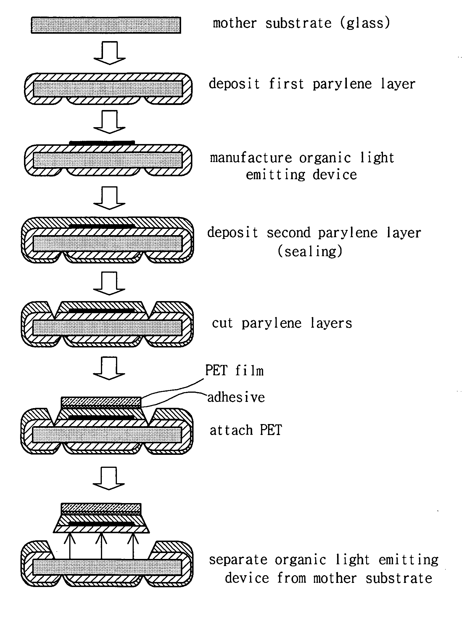
[0033] According to a method of manufacturing a device having a flexible substrate of the invention, glass is used as a mother substrate, a polymer layer, which is used as a substrate, is formed on the mother substrate by using a chemical vapor deposition method or a vacuum evaporation method, a device is formed, and finally, the substrate where the device is formed is separated from the mother substrate, such that a large-scale device having a flexible substrate can be manufactured. Further, as a substrate forming an organic light emitting device and a sealant are formed of the same material, the device is not bent due to stress generated from the device itself after the device is manufactured.

Problems solved by technology

In terms of price and performance, the organic light emitting device is not more excellent than the LCD.
Therefore, it is difficult for the organic light emitting device to enter markets.
Here, there is a disadvantage when it is difficult to use a large-area substrate because the substrate may be bent during the process.
However, since the above-described methods manufacture the plastic substrates through injection or a laminating process, the surface of the plastic substrates is rough.
In addition, defects, such as dust formed when the plastic substrate is bonded to the mother substrate, have a fatal effect on life span of the organic light emitting device that is subsequently manufactured using vacuum evaporation.
However, this method is different from the first method in that the process is performed while rolling a long substrate.
However, this method does not reach a technical level sufficient to be applied to manufacture organic light emitting devices.
Because of the above-described reasons, even though research on the flexible organic light emitting devices has actively been made, significant results of commercialization thereof have not been reported.

Method used


Image

  • Method of manufacturing device having flexible substrate and device having flexible substrate manufactured using the same
  • Method of manufacturing device having flexible substrate and device having flexible substrate manufactured using the same
  • Method of manufacturing device having flexible substrate and device having flexible substrate manufactured using the same

Examples


first embodiment

[0040] Manufacturing organic light emitting device having flexible substrate according to first embodiment of the present invention

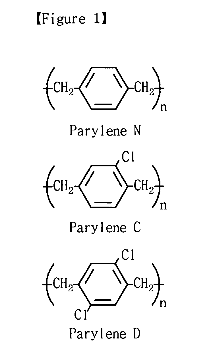
[0041] A glass substrate is used for a mother substrate, and parylene C is used for a substrate for manufacturing an organic light emitting device and a sealant.

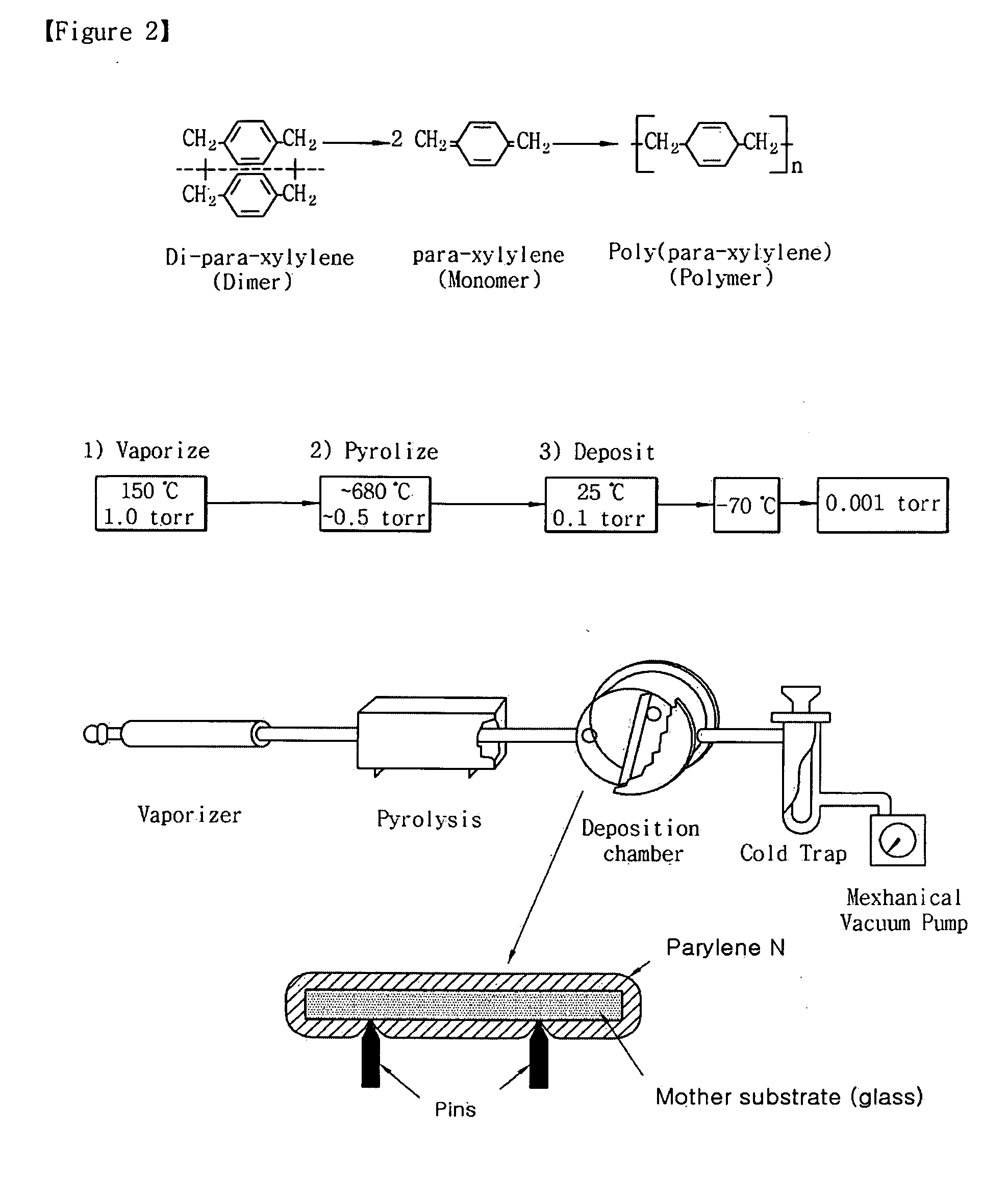
[0042] The glass substrate, which is the mother substrate and has a size of 100×100 mm2, is initially cleaned using acetone and methanol. Then, the cleaned glass substrate is put into a parylene deposition apparatus. A first parylene layer is deposited to a thickness of 30 μm using a vapor deposition method in the parylene deposition apparatus. The parylene is deposited over the entire surface of the glass substrate, except for point contacts of three pins for supporting the glass substrate, which is the mother substrate. FIG. 2 is a conceptual view showing a parylene deposition process. After the first parylene layer is deposited over the mother substrate, an organic light emitting device is m...

second embodiment

[0047] Manufacturing device having flexible substrate according to second embodiment of the invention.

[0048] According to the first embodiment, the first and second parylene layers have a thickness of 30 μm, respectively. The device having a total thickness of 60 μm can be very easily bent, and is rather susceptible to damage. As a method of complementing this disadvantage and reducing deposition time of thick parylene layers, a flexible polymer film or a metal film may be additionally attached to one side or both sides of the device.

[0049] A method of manufacturing a device according to this embodiment is the same as the method according to the first embodiment until a first parylene layer, an organic light emitting device, a second parylene layer are formed on a mother substrate, and then the two parylene layers are cut. Here, the first parylene layer and the second parylene layer have a thickness of 10 μm, respectively. The parylene layers do not need to be thick because an add...

third and forth embodiment

[0054] Organic lighting emitting device having a flexible substrate is prepared by same process in the first and second embodiment except parylene N is used instead of parylene C as sealant material. Same results were obtained in the first and second embodiment.


PUM


Abstract

The present invention relates to a method of manufacturing a device having a flexible substrate and a device having a flexible substrate manufactured using the method. According to the method of manufacturing a device having a flexible substrate of the invention, glass is used as a mother substrate, a polymer layer, which is used as a substrate, is formed on the mother substrate using a chemical vapor deposition method or a vacuum evaporation method, a device is formed, and finally, the substrate where the device is formed is separated from the mother substrate, such that a large-scale device having a flexible substrate can be manufactured. Further, as a substrate forming an organic light emitting device and a sealant are formed of the same material, the device is not bent due to stress generated from the device itself after the device is manufactured.

Description

TECHNICAL FIELD [0001] The present invention relates to a method of manufacturing a device having a flexible substrate and a device having a flexible substrate manufactured using the same. [0002] This application claims priority benefits from Korean Patent Application No. 10-2005-0103899, filed on Nov. 1, 2005, the entire contents of which are fully incorporated herein by reference. BACKGROUND ART [0003] In general, an organic light emitting device (OLED) includes two electrodes (an anode and a cathode) and at least one organic layer interposed between the two electrodes. In the organic light emitting device having this structure, when a voltage is applied between the two electrodes, holes from the anode and electrons from the cathode are injected into the organic layer. The electrons and the holes are recombined in the organic layer to thereby form excitons. When the excitons drop to a ground state again, photons corresponding to the energy difference are emitted. According to this...

Claims


Application Information

Patent Timeline
IPC IPC(8): H01L21/00
CPCH01L51/003H01L51/5253H01L51/56H01L2227/326H01L2251/5338H10K71/80H10K59/1201H10K2102/311H10K71/00H10K50/844H05B33/10H05B33/22
Inventor LEE, YOUNG CHULLEE, JAE SEUNGNOH, JEOUNG KWEN
Owner LG DISPLAY CO LTD
Learn More