Semiconductor device and method of manufacturing the same

a semiconductor and semiconductor technology, applied in the direction of semiconductor/solid-state device manufacturing, semiconductor devices, electrical devices, etc., can solve the problems of low production yield, high probability of defective articles, and difficulty in sufficiently activating impurities, so as to reduce reverse leakage current, reduce the thickness of semiconductor substrates, and reduce the effect of reverse leakage curren

Active Publication Date: 2007-05-17
FUJI ELECTRIC CO LTD
View PDF4 Cites 61 Cited by
  • Summary
  • Abstract
  • Description
  • Claims
  • Application Information

AI Technical Summary

Benefits of technology

[0028] Semiconductor devices according to the embodiments of the invention exhibit an advantage that the reverse leakage current is decreased, the semiconductor device being fabricated by decreasing thickness of a semiconductor substrate by grinding, then performing ion implantation into such a ground surface and thermal activating an implanted element. Moreover, according to t

Problems solved by technology

Therefore, it is hard to sufficiently activate impurities.
However, such a diode or IGBT, which is fabricated by the method in which one surface of a semiconductor substrate is ground, and a cathode layer of the diode or a collector layer of the IGBT is formed on such a ground surface, exhibits a problem in that the probability of defective articles is high in measurement of electric characteristics in a wafer state before being cut into individual chips, that is, production yield is low.
The problem of generation of such a reverse leakage curr

Method used


Image

  • Semiconductor device and method of manufacturing the same
  • Semiconductor device and method of manufacturing the same
  • Semiconductor device and method of manufacturing the same

Examples


embodiment 1

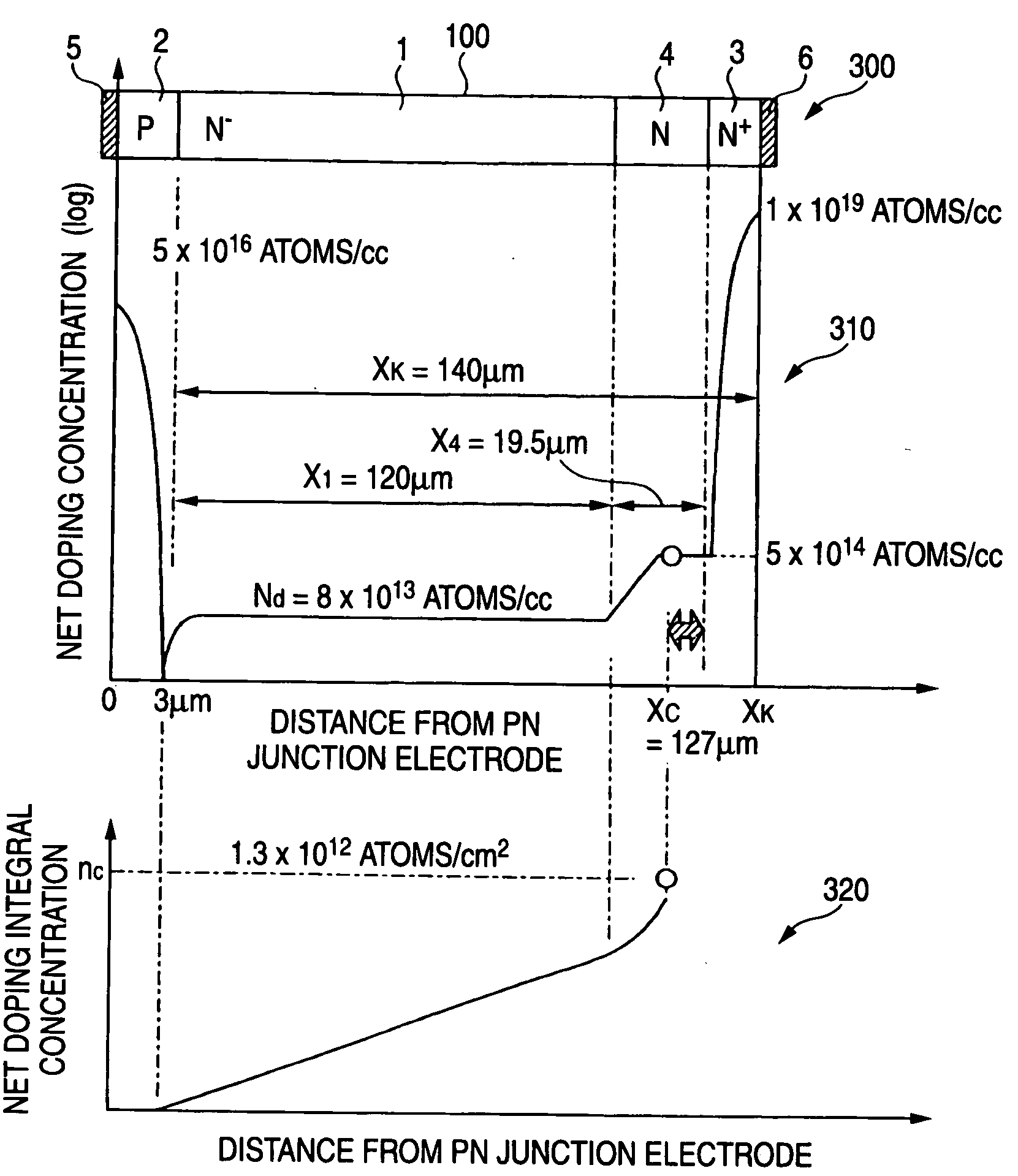
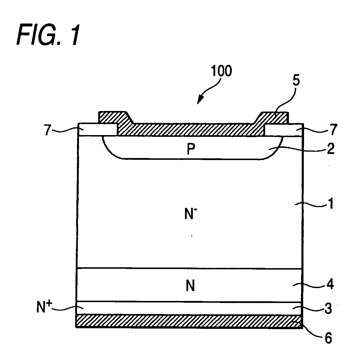
[0054]FIG. 1 shows a cross section view showing a configuration of a semiconductor device according to embodiment 1 of the invention. As shown in FIG. 1, the semiconductor device of the embodiment 1 is, for example, a diode 100 having an N− drift layer 1 as a first semiconductor layer, a P anode layer 2 as a second semiconductor layer, N+ cathode layer 3 as a third semiconductor layer, an N cathode buffer layer 4 as a fourth semiconductor layer, an anode electrode 5 as a first electrode, and a cathode electrode 6 as a second electrode.

[0055] The P anode layer 2 is provided in contact with the N− drift layer 1 at a side of one main surface of the N− drift layer 1. The N+ cathode layer 3 is provided at a side of the other main surface of the N− drift layer 1. The N cathode buffer layer 4 is provided between the N drift layer 1 and the N+ cathode layer 3, and contacted to both the N− drift layer 1 and the N+ cathode layer 3.

[0056] That is, the semiconductor device is in a structure w...

embodiment 2

[0108] In embodiment 2, the diode 100 shown in FIG. 1 is fabricated in a different procedure from that in the embodiment 1. A configuration of a diode of the embodiment 2 is the same as that of the diode 100 of the embodiment 1 shown in FIG. 1. In the following description, overlapped description with description in the embodiment 1 is omitted.

[0109]FIG. 16 shows an explanatory view showing an example of doping concentration of the diode of the embodiment 2. As shown in FIG. 16, in the embodiment 2, concentration distribution of the N cathode buffer layer 4 is not uniform unlike the embodiment 1, and for example, gradually reduced from a cathode side to an anode side. The N cathode buffer layer 4 having such concentration distribution is formed by, for example, diffusing selenium (Se) from the cathode side, as described later. In FIG. 16, indication of Se by an arrow means that the relevant portion (N cathode buffer layer 4) has selenium as a dopant. Similarly, a portion indicated ...

embodiment 3

[0119] In embodiment 3, the diode 100 shown in FIG. 1 is fabricated in a different procedure from that in the embodiment 1. A configuration of a diode of the embodiment 3 is the same as that of the diode 100 of the embodiment 1 shown in FIG. 1. In the following description, overlapped description with description in the example 1 is omitted.

[0120]FIG. 19 shows an explanatory view showing an example of doping concentration of the diode of the embodiment 3. As shown in FIG. 19, in the embodiment 3, concentration distribution of the N cathode buffer layer 4 is gradually reduced, for example, from a cathode side to an anode side, as the embodiment 2. Moreover, a broad buffer layer is formed in the N− drift layer 1, the buffer layer having impurity concentration being reduced with approaching an anode side and a cathode side from the center of the drift layer 1. Such a broad buffer layer and an effect of the layer are as disclosed in the JP-A-2003-318412.

[0121] In FIG. 19, indication o...


PUM


Abstract

A semiconductor device formed by decreasing thickness of a substrate by grinding, and performing ion implantation. In a diode in which a P anode layer and an anode electrode are formed at a side of a right face of an N drift layer, and an N+ cathode layer and a cathode electrode are formed at a side of a back face of the N drift layer, an N cathode buffer layer is formed thick compared with the N+-type cathode layer between the N-type drift layer and the N+ cathode layer, the buffer layer being high in concentration compared with the N drift layer, and low compared with the N+ cathode layer. When a reverse bias voltage is applied, a depletion layer is stopped in the middle of the N cathode buffer layer, and thus prevented from reaching the N+ cathode layer, so that the leakage current is suppressed.

Description

BACKGROUND OF THE INVENTION [0001] 1. Field of the Invention [0002] The present invention relates to a semiconductor device decreased in thickness by a backgrinding process of a semiconductor substrate, and a method of manufacturing the device. [0003] 2. Description of Related Art [0004] As a method of manufacturing a power semiconductor device such as a diode or an insulated gate bipolar transistor (hereinafter, referred to as IGBT), the following method is known. First, a semiconductor device is manufactured using a wafer such as silicon wafer while it has a large thickness. Then, the wafer is decreased in thickness to have a final thickness by grinding and etching, and then subjected to ion implantation and activation heat treatment (for example, refer to JP-T-2002-520885, where the term “JP-T” as used herein means a published Japanese translation of a PCT patent application). Such a manufacturing method is becoming mainstream in recent years. [0005] However, in this manufacturin...

Claims


Application Information

Patent Timeline
IPC IPC(8): H01L29/00H01L31/00
CPCH01L29/36H01L29/66136H01L29/861H01L29/868
Inventor NEMOTO, MICHIO
Owner FUJI ELECTRIC CO LTD
Why Eureka
Try Eureka