Silicon carbide Schottky diode and manufacturing method thereof

A technology of Schottky diodes and manufacturing methods, applied in semiconductor/solid-state device manufacturing, gaseous chemical plating, ion implantation plating, etc., can solve the problem of reverse breakdown voltage decrease, reverse leakage voltage increase, wafer Fragmentation and other problems, to achieve the effect of small reverse leakage current, large reverse breakdown voltage, and reduced fragmentation rate

Active Publication Date: 2020-05-22
FOUNDER MICROELECTRONICS INT
View PDF13 Cites 2 Cited by
  • Summary
  • Abstract
  • Description
  • Claims
  • Application Information

AI Technical Summary

Problems solved by technology

[0005] The purpose of the present invention is to provide a method for manufacturing silicon carbide Schottky diodes, aiming to solve the problem of wafer fragmentation and reverse leakage caused by excessive stress of silicon carbide wafers in the manufacturing process of existing silicon carbide Schottky diodes. Voltage increase, reverse breakdown voltage decrease, etc.

Method used


Image

  • Silicon carbide Schottky diode and manufacturing method thereof
  • Silicon carbide Schottky diode and manufacturing method thereof
  • Silicon carbide Schottky diode and manufacturing method thereof

Examples


Embodiment 1

[0096] see Figure 1-16 , this implementation 1 provides a method for manufacturing a silicon carbide Schottky diode, specifically comprising the following steps:

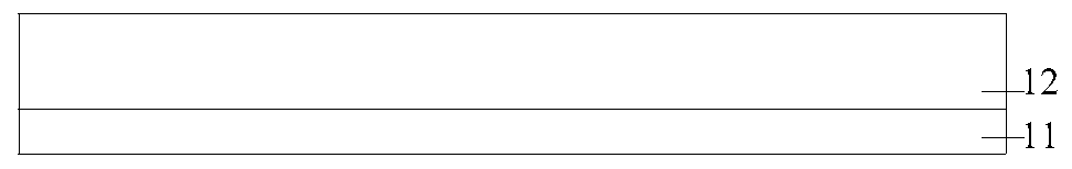
[0097] S1. Provide a silicon substrate 11, a silicon carbide epitaxial layer 12 is deposited on one surface of the silicon substrate 11, the thickness of the silicon substrate 11 is 500 μm, and the thickness of the silicon carbide epitaxial layer 12 is 30 μm; Pickling, washing, drying treatment. Subsequently, the exposed surface of the silicon substrate 11 is dry-etched with a photoresist coating, exposure and development process to etch an alignment overlay pattern with a depth of 1.5 μm and a width of 1.5 μm, and a conventional stripping process is used. Residual photoresist is removed, followed by pickling, washing with water, and drying for use.

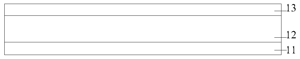
[0098] S2. Using the plasma-enhanced chemical vapor deposition method, deposit three times on the surface of the silicon carbide epitaxial layer 12 to form a silico...

Embodiment 2

[0116] see Figure 1-16 , this implementation 2 provides a method for manufacturing a silicon carbide Schottky diode, specifically comprising the following steps:

[0117] S1. Provide a silicon substrate 11, a silicon carbide epitaxial layer 12 is deposited on one surface of the silicon substrate 11, the thickness of the silicon substrate 11 is 800 μm, and the thickness of the silicon carbide epitaxial layer 12 is 20 μm; Pickling, washing, drying treatment. Subsequently, the exposed surface of the silicon substrate 11 is dry-etched with a photoresist coating, exposure and development process to etch an alignment overlay pattern with a depth of 1.5 μm and a width of 1.5 μm, and a conventional stripping process is used. Residual photoresist is removed, followed by pickling, washing with water, and drying for use.

[0118] S2. Using the plasma-enhanced chemical vapor deposition method, deposit three times on the surface of the silicon carbide epitaxial layer 12 to form a silico...

Embodiment 3

[0136] see Figure 1-16 , this implementation 3 provides a method for manufacturing a silicon carbide Schottky diode, specifically comprising the following steps:

[0137] S1. Provide a silicon substrate 11, a silicon carbide epitaxial layer 12 is deposited on one surface of the silicon substrate 11, the thickness of the silicon substrate 11 is 500 μm, and the thickness of the silicon carbide epitaxial layer 12 is 50 μm; Pickling, washing, drying treatment. Subsequently, the exposed surface of the silicon substrate 11 is dry-etched with a photoresist coating, exposure and development process to etch an alignment overlay pattern with a depth of 1.5 μm and a width of 1.5 μm, and a conventional stripping process is used. Residual photoresist is removed, followed by pickling, washing with water, and drying for use.

[0138] S2. Using the plasma-enhanced chemical vapor deposition method, deposit five times on the surface of the silicon carbide epitaxial layer 12 to form a silicon...


PUM

PropertyMeasurementUnit
thicknessaaaaaaaaaa
thicknessaaaaaaaaaa
thicknessaaaaaaaaaa

Abstract

The invention relates to the technical field of Schottky diodes, and particularly provides a silicon carbide Schottky diode and a manufacturing method thereof. The manufacturing method of the siliconcarbide Schottky diode comprises the following steps that: when a mask layer, an isolation dielectric layer, a Schottky metal film layer and a passivation layer are formed, deposition is carried out for several times, so that the possibility of stress concentration is reduced, and the stress distribution is adjusted. The silicon carbide Schottky diode obtained through adoption of the manufacturingmethod has the advantages of being high in finished product percent of pass, small in reverse leakage current, large in reverse breakdown voltage, high in reliability, long in service life and the like.

Description

technical field [0001] The invention belongs to the technical field of Schottky diodes, in particular to a silicon carbide Schottky diode and a manufacturing method thereof. Background technique [0002] As a new generation of wide bandgap semiconductor material, silicon carbide (SiC) has extremely excellent performance in the field of power semiconductors, and is the frontier and future direction of the development of power semiconductor devices. SiC (silicon carbide) is a compound semiconductor material composed of silicon (Si) and carbon (C), which has superior electrical properties, including a wide band gap (2.3-3.3eV), which is 3 times that of Si; high breakdown Field strength (0.8E16~3E16V / cm), 10 times that of Si; high saturation drift velocity (2E7cm / s), 2.7 times that of Si; and high thermal conductivity (4.9W / cm K), about 3.2 times that of Si . These characteristics make silicon carbide materials have excellent characteristics such as large band gap, high breakd...

Claims


Application Information

Patent Timeline
Patent Type & Authority Applications(China)
IPC IPC(8): H01L21/329H01L29/872H01L29/16H01L21/265C23C16/513C23C16/40C23C16/34C23C14/58C23C14/48C23C14/34C23C14/18C23C14/04
CPCH01L29/872H01L29/66143H01L29/1608H01L21/26513C23C16/402C23C16/345C23C16/513C23C14/042C23C14/185C23C14/5806C23C14/34C23C14/48C23C14/18Y02P70/50
Inventor 贺冠中
Owner FOUNDER MICROELECTRONICS INT
Why Eureka
Try Eureka