Display device and fabricating method thereof

a technology of a display device and a fabrication method, which is applied in the direction of discharge tube/lamp details, organic semiconductor devices, discharge tubes luminescnet screens, etc., can solve the problem of difficult to efficiently apply a common voltage, and achieve the effect of improving the contrast ratio

Active Publication Date: 2007-05-17
SAMSUNG DISPLAY CO LTD
View PDF4 Cites 144 Cited by
  • Summary
  • Abstract
  • Description
  • Claims
  • Application Information

AI Technical Summary

Benefits of technology

[0009] Accordingly, it is an aspect of the present invention to provide a display de

Problems solved by technology

However, the resistance of the thin common electrode is relatively

Method used


Image

  • Display device and fabricating method thereof
  • Display device and fabricating method thereof
  • Display device and fabricating method thereof

Examples


first embodiment

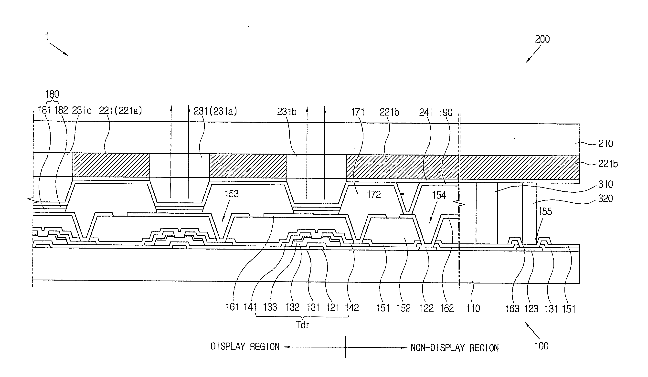
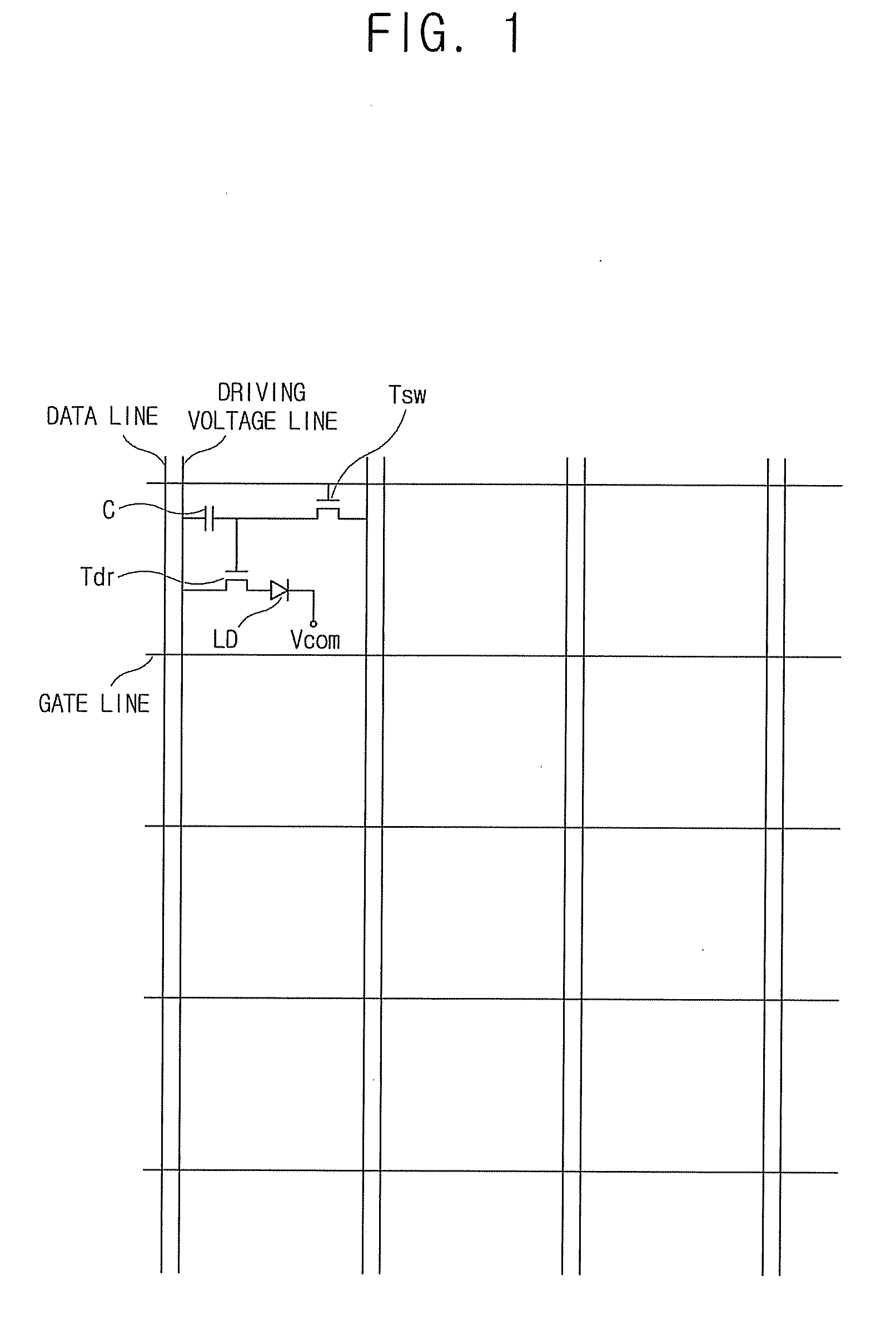
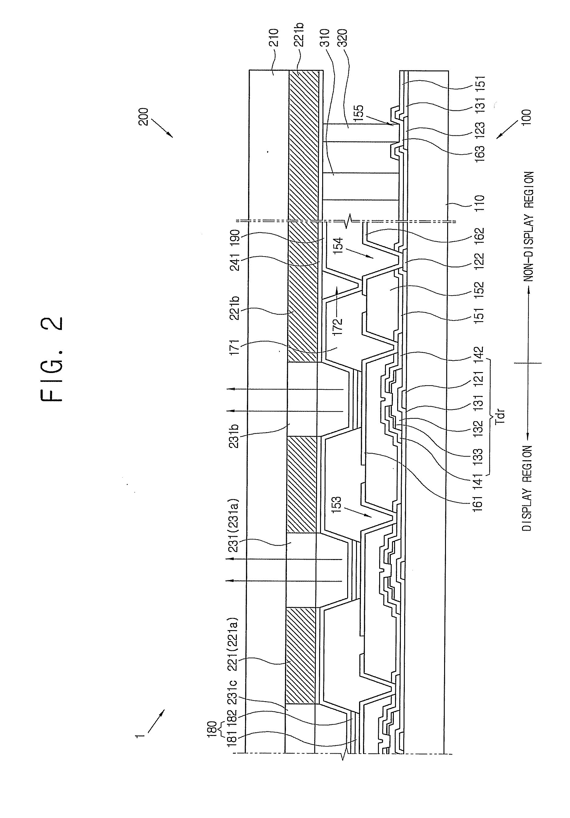
[0049] Referring to FIG. 1, a display device 1 includes a plurality of signal lines.

[0050] The signal lines include a gate line to transmit a scan signal, a data line to transmit a data signal, and a driving voltage line to apply a driving voltage. The data line and the driving voltage line are adjacent to and arranged in parallel with each other. Further, the gate line intersects both the data line and the driving voltage line.

[0051] A pixel includes an organic light emitting device LD, a switching transistor Tsw, a driving transistor Tdr, and a capacitor C.

[0052] The driving transistor Tdr has a control terminal connected to the switching transistor Tsw, an input terminal connected to the driving voltage line, and an output terminal connected to the organic light emitting device LD.

[0053] The organic light emitting device LD has an anode connected to the output terminal of the driving transistor Tdr, and a cathode connected to a common voltage Vcom. The organic light emitting ...

second embodiment

[0097] Referring to FIG. 5, an organic emission layer 182 may include one of three sub-layers 182a, 182b and 182c, which differ in the color of light emitted therefrom; e.g., they may emit red, blue and green light, respectively. The organic emission layer 182 may include a poly fluorene derivative; a (poly)paraphenylenevinylene derivative; a polyphenylene derivative; polyvinylcarbazole; and poly thiophene. The polymer materials listed above may be doped with a perylene pigment; a rothermine pigment; rubrene; perylene; 9,10-diphenylanthracene; tetraphenylbutadiene; Nile red; coumarine 6; Quinacridone, or other substances with similar characteristics. Meanwhile, the transparent organic layer 251 is formed on the organic emission layer 182. The organic layer 251 is colorless and includes one of benzocyclobutene (“BCB”) series, olefin series, acrylic resin series, polyimide series, and fluoropolymer.

third embodiment

[0098] Referring to FIG. 6, according to the present invention, a conductive layer 330 is formed between the common electrode 190 and the auxiliary electrode 241. The conductive layer 330 includes a conductive polymer and enhances the electric connection between the common electrode 190 and the auxiliary electrode 241. As an example of the conductive polymer, there are poly pyrrole, poly aniline, poly thiophene, and other substances with similar characteristics. The conductive layer 330 also includes conductive particles 331. Here, the conductive particles 331 comprise nickel or silver.

[0099] The conductive layer 330 can either be formed on the first substrate 100 or the second substrate 200 while being fabricated.


PUM


Abstract

A display device includes a thin film transistor formed on a first insulating substrate, a first electrode electrically connected with the thin film transistor, an emission layer formed on the first electrode, a second electrode formed on the emission layer, an auxiliary electrode shaped like a mesh to at least partially expose the first electrode, the auxiliary electrode being electrically connected with the second electrode and receiving a common voltage therefrom, and a second insulating substrate placed on the auxiliary electrode. The exemplary embodiments of a display device, and a method of manufacturing the same, according to the present invention can apply a common voltage efficiently throughout the display and have an improved contrast ratio.

Description

[0001] This application claims priority to Korean Patent Application No. 2005-0109142, filed on Nov. 15, 2005 and Korean Patent Application No. 2006-0090046, filed on Sep. 18, 2006 and all the benefits accruing therefrom under 35 U.S.C. §119, the contents of which in its entirety are herein incorporated by reference. BACKGROUND OF THE INVENTION [0002] (a) Field of the Invention [0003] The present invention relates to a display device and a fabricating method thereof, and more particularly, to a display device and a fabricating method thereof, which can efficiently apply a common voltage across the display and has an improved contrast ratio. [0004] (b) Description of the Related Art [0005] Among flat panel displays, an organic light emitting diode (“OLED”) display has recently attracted attention because it is driven with a low voltage; is both thin and light; has a wide viewing angle; has a relatively short response time; and various other attractive and desirable features. OLED dis...

Claims


Application Information

Patent Timeline
IPC IPC(8): H05B33/00
CPCH01L27/322H01L27/3276H01L51/5203H01L51/5284H01L2251/5315H10K59/38H10K59/131H10K50/865H10K2102/3026H10K59/805H10K50/805
Inventor JUNG, JAE-HOONLEE, SUNG-SOOCHOI, JI-HYE
Owner SAMSUNG DISPLAY CO LTD
Why Eureka
Try Eureka