Method for operating single-poly non-volatile memory device

a non-volatile memory and single-poly technology, applied in semiconductor devices, digital storage, instruments, etc., can solve the problems of increasing costs, affecting the performance of memory devices, and inevitably delayed schedules, and achieve the effect of low voltag

Active Publication Date: 2007-05-17
EMEMORY TECH INC
View PDF10 Cites 36 Cited by
  • Summary
  • Abstract
  • Description
  • Claims
  • Application Information

AI Technical Summary

Benefits of technology

[0017] It is one aspect of the present invention to provide a double-channel single-poly erasable and programmable read-only memory device and a method of low voltage operation for its programming, reading and erasing operations to solve the problems addressed above.

Problems solved by technology

On the other hand, in the advanced logic process, the embedding of double-poly non-volatile memory will greatly increase the cost and changes the electrical characteristics of devices because of additional thermal budget, followed by re-adjusting the characteristics of the devices back to origin device targets, so the schedule will be inevitably delayed.
The conventional single-poly non-volatile memory still has a lot of disadvantages that need improvement.
First, the conventional single-poly non-volatile memory takes more wafer area.
So far, no desirous solution is proposed for further miniaturizing the size of the single-poly one-time programmable memory with respect to the semiconductor logic process of 90 nm or less.
Take the 90 nm technology for example, the thickest oxide layer is about 50 to 60 Å. It is a great challenge for the use of floating gate technique to produce multi-time programmable single-poly non-volatile memory for the reason that the insufficient tunnel oxide thickness deteriorates long term charge retention.
On the other hand, it is not compatible with the current logic process to increase the thickness of the oxide layer.
Because the required operational voltage is much higher than the VCC voltage (for example 3.3V VCC supply voltage for input / output circuits) supplied, it results in the serious problem of reliability for the gate oxide layers of tens of Å in the more advanced nano-process.

Method used


Image

  • Method for operating single-poly non-volatile memory device
  • Method for operating single-poly non-volatile memory device
  • Method for operating single-poly non-volatile memory device

Examples


Embodiment Construction

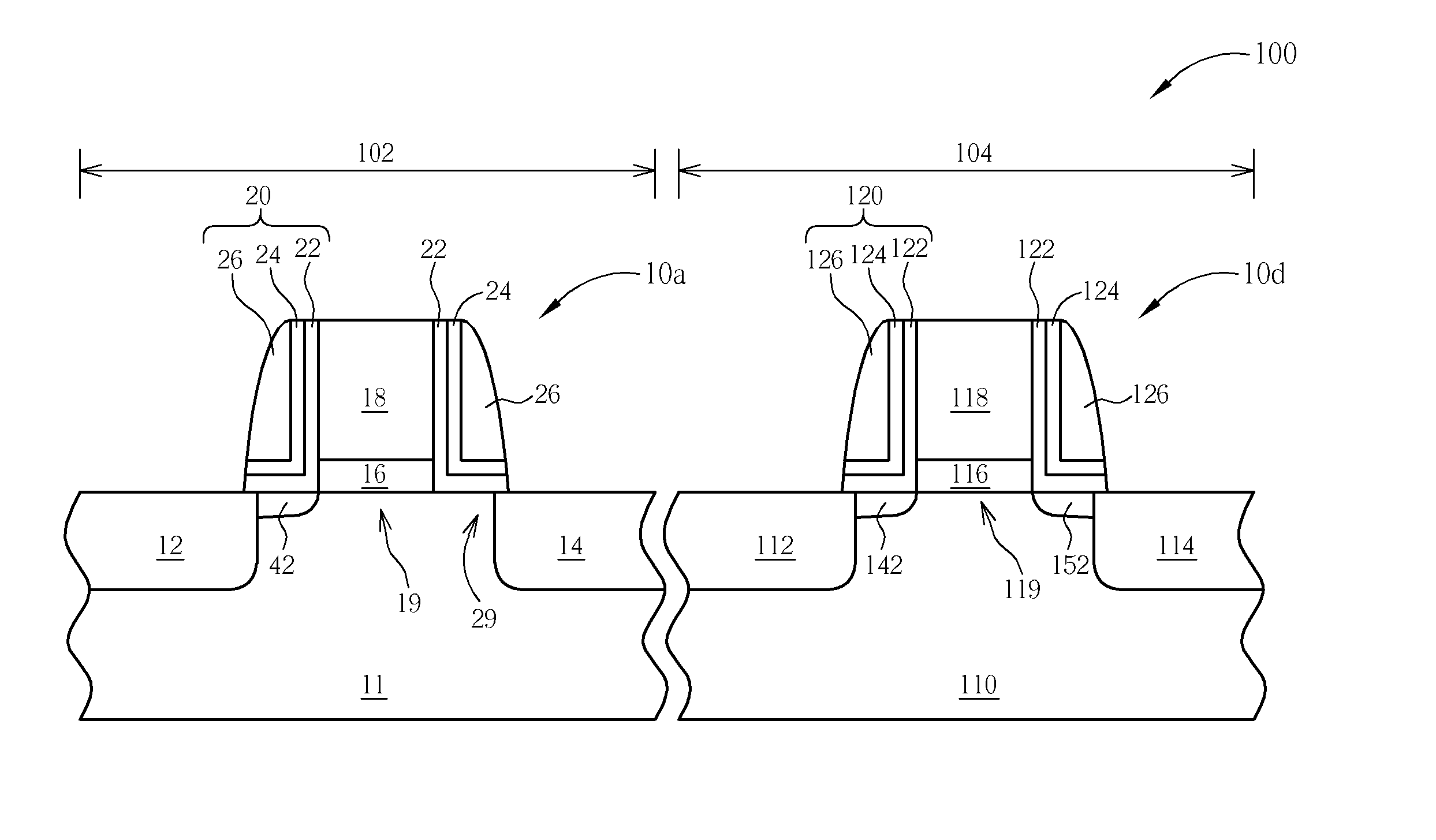
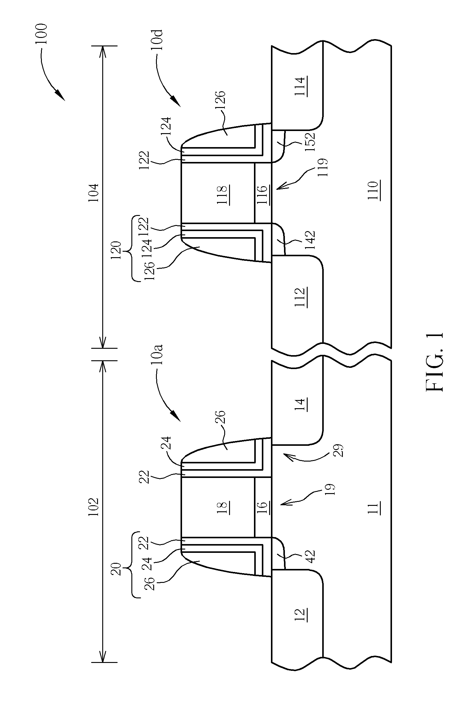
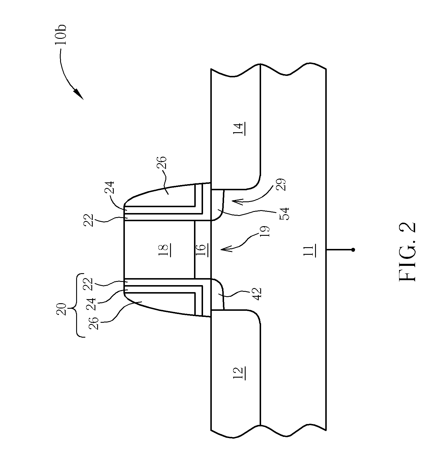
[0060] The present invention relates to a structure of a single-poly non-volatile memory unit and the method of operation. In particular, the structure of a single-poly non-volatile memory unit of the present invention is completely compatible with the current semiconductor logic process of 90 nm or less and with the trend of miniaturization of the elements of the next generation.

[0061] The ONO stacking layers usually serve as the spacer in the semiconductor logic process of 0.18 μm or less for the reasons that first, using SiN as the material for the spacer is better than the use of SiO2 in order to prevent the case that salicide is formed on the spacer to electrically connect the source / drain to cause element failure, and second, it is possible that the structure and the reliability of elements are sabotaged by the approach of contact holes of the source to the poly-Si to result in the contact holes going through the spacer due to the misalignment of the contact mask and the gate...


PUM


Abstract

A single-poly non-volatile memory cell that is fully compatible with nano-scale semiconductor manufacturing process is provided. The single-poly non-volatile memory cell includes an ion well, a gate formed on the ion well, a gate dielectric layer between the gate and the ion well, a dielectric stack layer on sidewalls of the gate, a source doping region and a drain doping region. The dielectric stack layer includes a first oxide layer deposited on the sidewalls of the gate and extends to the ion well, and a silicon nitride layer formed on the first oxide layer. The silicon nitride layer functions as a charge-trapping layer.

Description

CROSS REFERENCE TO RELATED APPLICATIONS [0001] This application claims the benefit of U.S. provisional application No. 60 / 597,210 filed Nov. 17, 2005 and U.S. provisional application No. 60 / 743,630 filed Mar. 22, 2006.BACKGROUND OF THE INVENTION [0002] 1. Field of the Invention [0003] The present invention relates to a method of operation for a non-volatile memory device. In particular, the present invention relates to double-channel single-poly non-volatile memory devices with gate channels and spacer channels and a method to change the threshold voltage of the spacer channels, wherein the single-poly non-volatile memory device has an asymmetric lightly doped drain (LDD) region. [0004] 2. Description of the Prior Art [0005] Currently, non-volatile memory is one of the most popular electronic storage media for saving information. One of the most important features of all is that the information stored in the non-volatile memory will not disappear once the power supply is cut off. Ge...

Claims


Application Information

Patent Timeline
Patent Type & Authority Applications(United States)
IPC IPC(8): G11C16/04
CPCG11C16/0425G11C16/0466G11C16/0475H01L21/28273H01L21/28282H01L27/105H01L27/115H01L27/11521H01L27/11568H01L29/42324H01L29/4234H01L29/42368H01L29/513H01L29/6656H01L29/66659H01L29/66825H01L29/66833H01L29/7835H01L29/7887H01L29/792H01L29/7923H01L29/40114H01L29/40117H10B43/30H10B69/00H10B41/30
Inventor WANG, SHIH-CHENCHEN, HSIN-MINGLU, CHUN-HUNGHO, MING-CHOUSHEN, SHIH-JYEHSU, CHING-HSIANG
Owner EMEMORY TECH INC
Why Eureka
Try Eureka