Printed wiring board, its manufacturing method, and circuit device

a manufacturing method and printed wiring technology, applied in the direction of printed circuit aspects, conductive pattern reinforcement, insulation substrate metal adhesion improvement, etc., can solve the problems of wiring pattern producing a printed wiring board liable to warpage, copper foil having any smaller thickness is extremely difficult to handle, and copper foil having any smaller thickness is extremely difficult to manufacture. achieve long-term stability, prevent the change of resistance between wires, and improve the effect of electrical resistan

Active Publication Date: 2007-05-17
HEFEI ESWIN MATERIALS TECH CO LTD
View PDF10 Cites 36 Cited by
  • Summary
  • Abstract
  • Description
  • Claims
  • Application Information

AI Technical Summary

Benefits of technology

[0016] The printed wiring board manufacturing process according to the invention eliminates the residual metals combined with the superficial polyimide of the insulating polyimide film exposed from the wiring pattern, together with the superficial surface of the insulating polyimide film. Consequently, the surface of the insulating polyimide film exposed from the wiring pattern is cut to a depth of 1 to 100 nm from the surface level, and the metals present in the insulating film surface are removed together. Accordingly, the insulating film between wires can attain its inherent

Problems solved by technology

Accordingly, production of the copper-clad laminate inevitably involves the handling of single copper foil.
The copper foil having any smaller thickness is extremely difficult to handle such that it must be fixed on a support.
When a copper-clad laminate includes such an extremely thin copper foil that is bonded to an insulating film with an adhesive, fabrication of a wiring pattern produces a printed wiring board that is liable to warpage due to thermal shrinkage of the adhesive that bonds the copper foil.
It has been increasingly difficult to meet such printed wiring board needs with the above three-layer copper-clad lami

Method used


Image

  • Printed wiring board, its manufacturing method, and circuit device
  • Printed wiring board, its manufacturing method, and circuit device
  • Printed wiring board, its manufacturing method, and circuit device

Examples


example 1

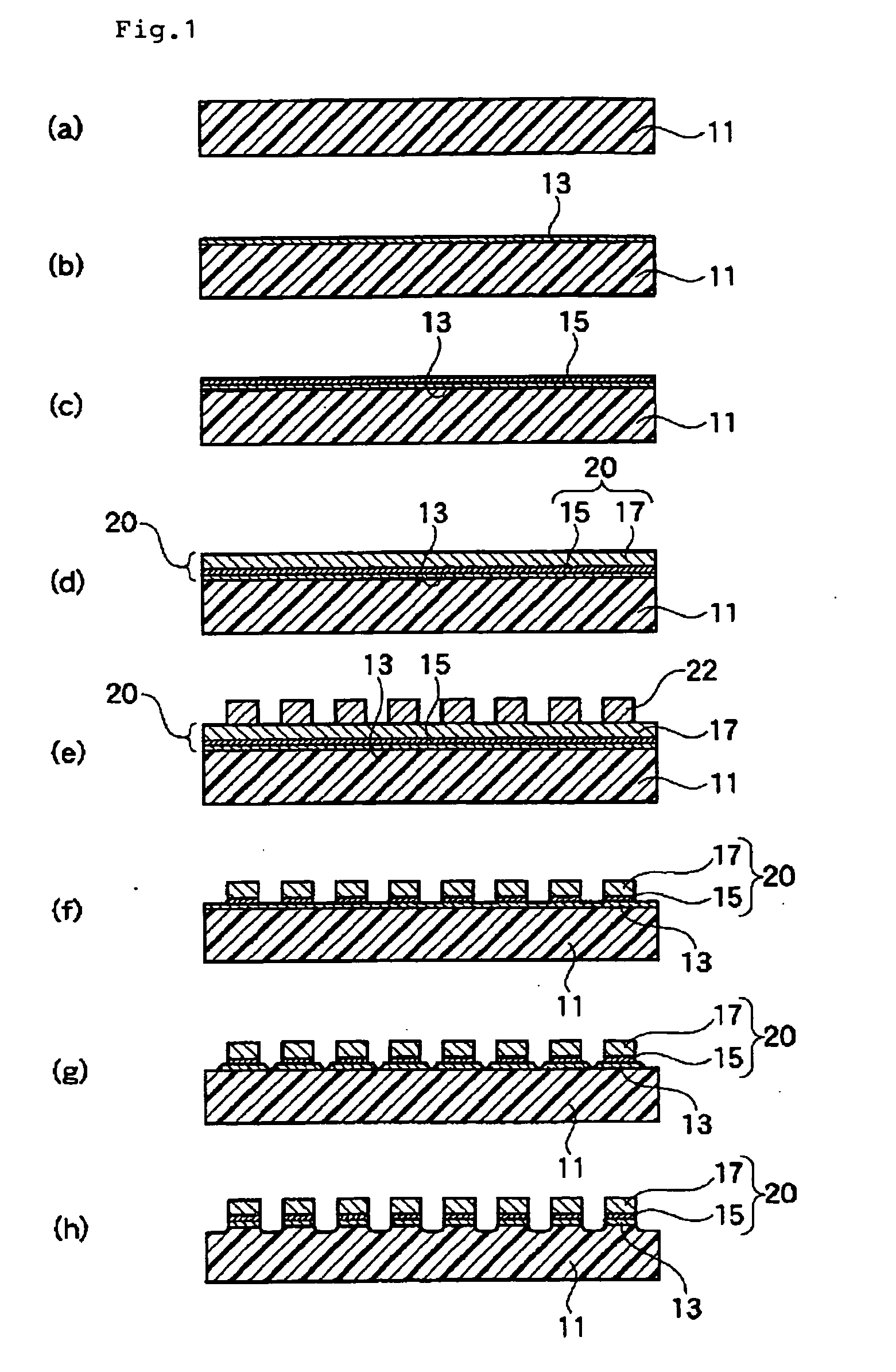
[0073] A polyimide film (UPILEX S, manufactured by UBE INDUSTRIES, LTD.) having an average thickness of 50 μm was roughened on one surface by reverse sputtering. Subsequently, a nickel-chrome alloy layer was sputtered in an average thickness of 40 nm under the following conditions to prepare a base metal layer.

[0074] The sputtering conditions were such that the 50 μm-thick polyimide film was treated at 100° C. and 3×10⁻⁵ Pa for 10 minutes, followed by degasification, and a chrome-nickel alloy was sputtered at 100° C. and 0.5 Pa.

[0075] On the base metal layer, copper was sputtered at 100° C. and 0.5 Pa in an average thickness of 300 nm.

[0076] The sputtered copper layer was electroplated with copper, and an electrolytic copper layer (electroplated copper layer) having a thickness of 8 μm was formed.

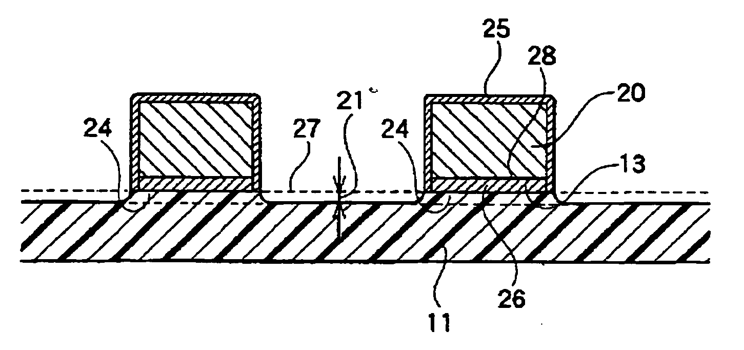
[0077] The copper layer (conductive metal layer) was coated with a photosensitive resin, and the resin was photoexposed and developed to produce comb-shaped wiring patterns having wire ...

example 2

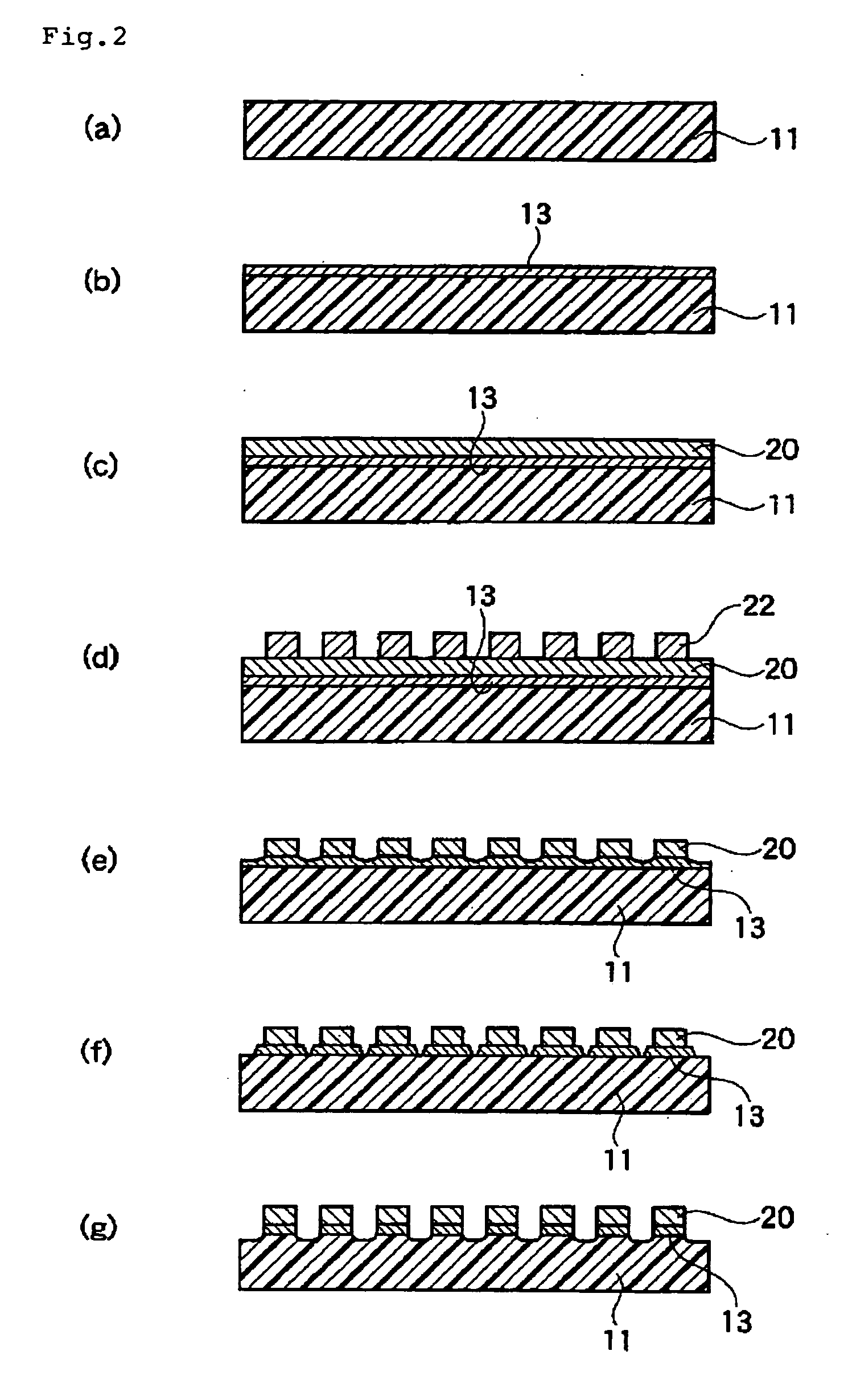
[0083] A polyimide film (UPILEX S, manufactured by UBE INDUSTRIES, LTD.) having an average thickness of 50 μm was roughened on one surface by reverse sputtering. Subsequently, a nickel-chrome alloy layer was sputtered in an average thickness of 40 nm under the following conditions to prepare a base metal layer.

[0084] The sputtering conditions were such that the 50 μm-thick polyimide film was treated at 100° C. and 3×10⁻⁵ Pa for 10 minutes, followed by degasification, and a chrome-nickel alloy was sputtered at 100° C. and 0.5 Pa.

[0085] The base metal layer sputtered as described above was electroplated with copper, and a conductive metal layer (electroplated copper layer) having a thickness of 8 μm was formed.

[0086] The conductive metal layer was coated with a photosensitive resin, and the resin was photoexposed and developed to produce comb-shaped wiring patterns having wire pitches of 30 μm (wire width: 15 μm, space width: 15 μm). The patterns were used as masks, and the copper ...

example 3

[0091] A polyimide film (UPILEX S, manufactured by UBE INDUSTRIES, LTD.) having an average thickness of 75 μm was roughened on one surface by reverse sputtering. Subsequently, a nickel-chrome alloy layer was sputtered in an average thickness of 30 nm under the same conditions as in Example 1 to prepare a base metal layer.

[0092] On the base metal layer, copper was sputtered in an average thickness of 200 nm under the conditions as described in Example 1.

[0093] The sputtered copper layer was electroplated with copper, and a conductive metal layer of electrolytic copper having a thickness of 8 μm was formed.

[0094] The conductive metal layer was coated with a photosensitive resin, and the resin was photoexposed and developed to produce comb-shaped wiring patterns having wire pitches of 30 μm. The patterns were used as masks, and the conductive metal layer was etched with a 12% cupric chloride etching solution containing 100 g / l of HCl for 30 seconds. Thus, wiring patterns were produc...


PUM


Abstract

A printed wiring board manufacturing process comprises forming a conductive metal layer on at least one surface of an insulating film with a sputtered metal layer in between, selectively etching the conductive metal layer and the sputtered metal layer to produce a wiring pattern, treating the laminated film with a first treatment liquid capable of dissolving nickel of the sputtered metal layer, and treating with a second treatment liquid capable of dissolving chrome of the sputtered metal layer and also capable of eliminating the sputtered metal layer in the insulating film to remove a superficial surface of the insulating film exposed from the wiring pattern together with the residual sputtered metals in the superficial surface. A printed wiring board comprises an insulating film and a wiring pattern, wherein the insulating film in an area exposed from the wiring pattern has a thickness smaller by 1 to 100 nm than that of an area under the wiring pattern. The process eliminates the sputtered metals combined with the insulating film together with the superficial surface of the insulating film, and therefore the insulating film surface between wires does not contain any residual metals and a short circuit between wires is prevented.

Description

FIELD OF THE INVENTION [0001] The present invention relates to a printed wiring board in which a wiring pattern is formed directly on a polyimide film without any intermediate adhesive layer, a process for manufacturing the printed wiring board, and a circuit device obtained by mounting an electronic component on the printed wiring board. More particularly, the invention relates to a printed wiring board that has a two-layer substrate including a base of a polyimide film and a metal layer on a surface of the insulating base, and the invention relates to a manufacturing process of the printed wiring board and a circuit device obtained by mounting an electronic component on the printed wiring board. BACKGROUND OF THE INVENTION [0002] Printed wiring board fabrication generally employs a copper-clad laminate produced by laminating a copper foil on a surface of an insulating film such as a polyimide film by means of an adhesive. [0003] To produce the copper-clad laminate, the copper foil...

Claims


Application Information

Patent Timeline
IPC IPC(8): H01L21/82H01L27/10H05K3/00H05K3/06H05K3/16H05K3/24H05K3/26H05K3/38
CPCH05K3/002H05K3/06H05K3/26H05K2203/1476H05K2201/0338H05K2201/0761H05K3/388H05K3/02
Inventor KATAOKA, TATSUOAKASHI, YOSHIKAZUIGUCHI, YUTAKA
Owner HEFEI ESWIN MATERIALS TECH CO LTD
Why Eureka
Try Eureka