Systems And Methods For Forming Integrated Circuit Components Having Matching Geometries

Inactive Publication Date: 2007-05-17
TOPPAN PHOTOMASKS INC
View PDF4 Cites 0 Cited by
  • Summary
  • Abstract
  • Description
  • Claims
  • Application Information

AI Technical Summary

Benefits of technology

[0008] One advantage of the present disclosure is that systems and methods may be provided for forming critical-geometry integrated circuit components having substantially identical geometries. In particular, by using a single pattern geometry on a photomask to form multiple instances of a particular integrated circuit component onto different locations of a die, geometric differences between the individual integrated cir

Problems solved by technology

However, various factors often cause imperfections and inconsistencies in the geometries of integrated circuit components formed in a semiconductor wafer, including imperfections in the geometries formed in a photomask used in the formation of the integrated circuit components, imperfections associated with the lithographic imaging of the integrated circuit components, imperfec

Method used


Image

  • Systems And Methods For Forming Integrated Circuit Components Having Matching Geometries
  • Systems And Methods For Forming Integrated Circuit Components Having Matching Geometries
  • Systems And Methods For Forming Integrated Circuit Components Having Matching Geometries

Examples


Example

[0018] Example embodiments of the present invention and their advantages are best understood by reference to FIGS. 1 through 5, where like numbers are used to indicate like and corresponding parts.

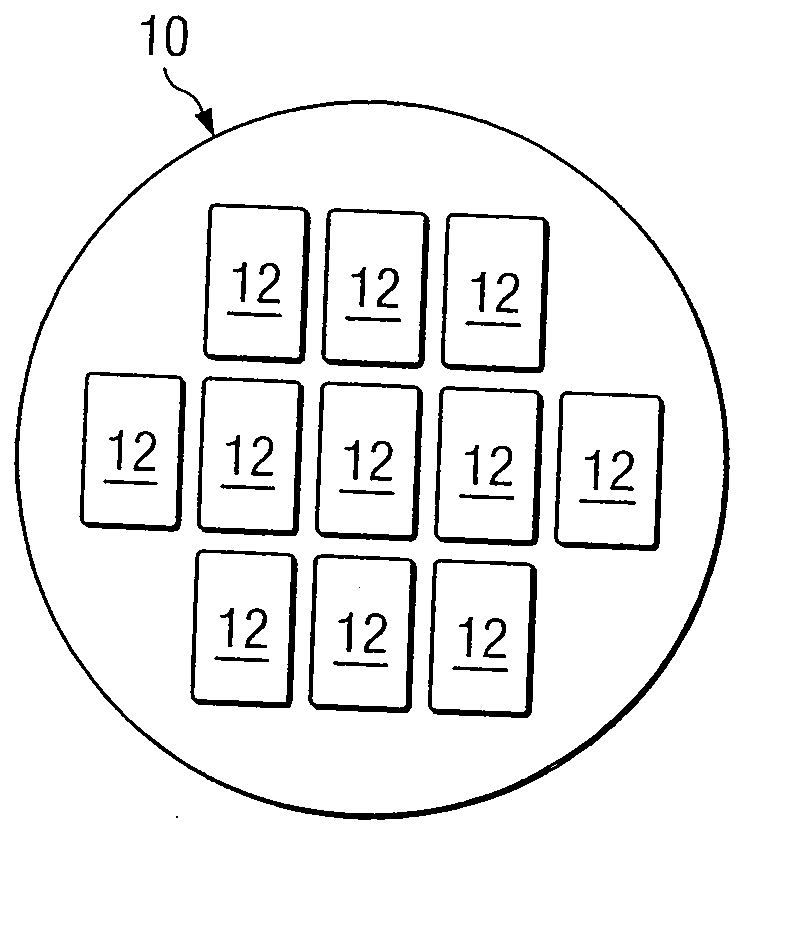
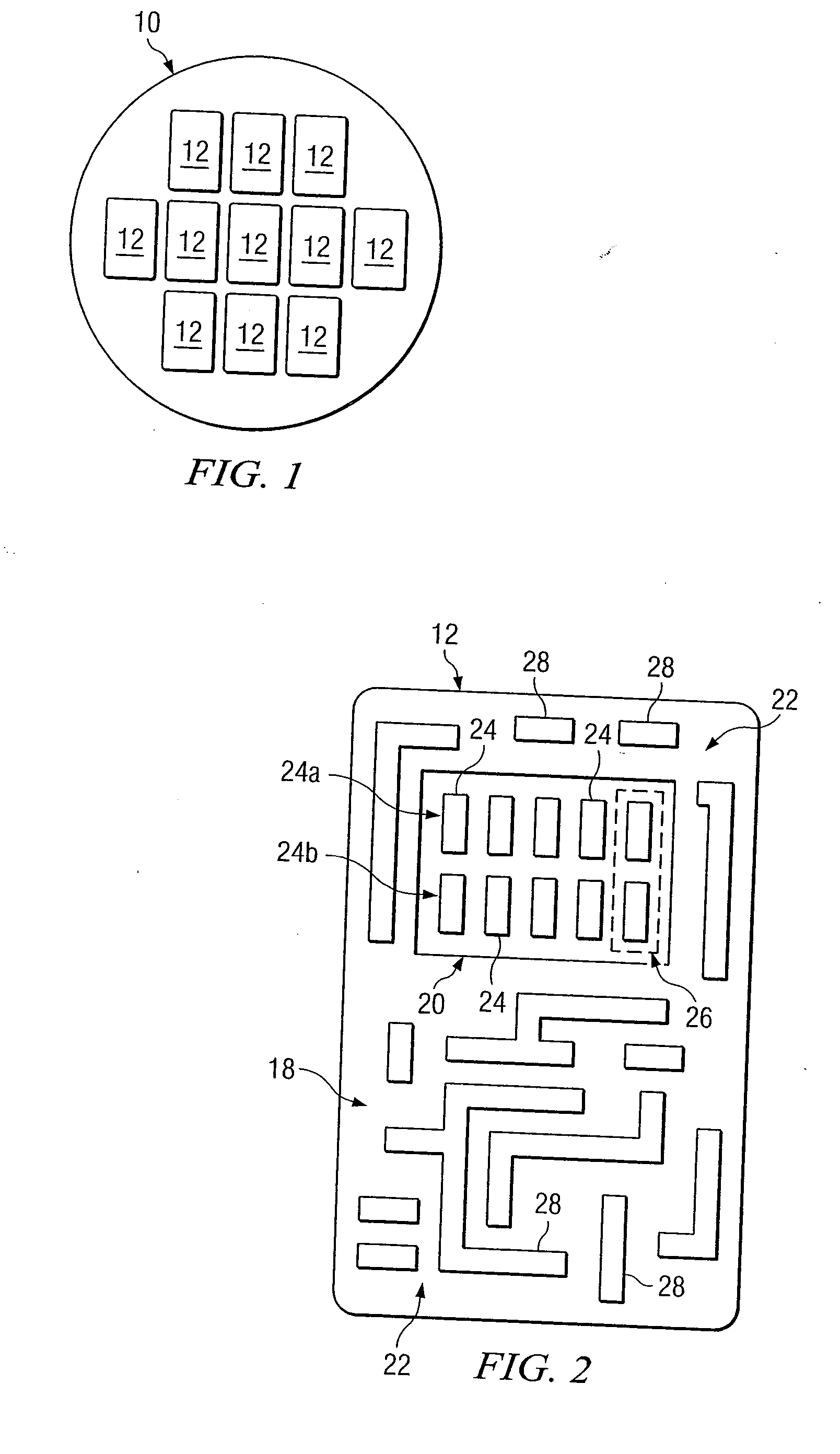
[0019]FIG. 1 illustrates a top view of an example semiconductor wafer 10 according to one embodiment of the invention. Semiconductor wafer 10 may include a plurality of dies, or chips, 12, each including one or more integrated circuits that include a variety of integrated circuit components. Semiconductor wafer 10 may comprise a thin, circular slice of single-crystal semiconductor material suitable for the manufacturing of semiconductor devices and / or integrated circuits. Semiconductor wafer 10 may include any suitable number of dies 12, which may be physically separated from each other after the integrated circuits have been formed in individual dies 12.

[0020]FIG. 2 illustrates a single one of dies 12 of semiconductor wafer 10, which may include integrated circuit components formed acco...


PUM


Abstract

In a particular embodiment, a method of forming integrated circuit components is provided. A first photomask is formed, the first photomask including a first mask component having a first geometry corresponding to a first type of integrated circuit component. A first lithography process is performed to transfer the first geometry of the first mask component of the first photomask to a first location on a first die on a semiconductor wafer to form a first integrated circuit component of the first type of integrated circuit component on the first die. A second lithography process is performed to transfer the first geometry of the first mask component of the first photomask to a second location on the first die on the semiconductor wafer to form a second integrated circuit component of the first type of integrated circuit component on the first die.

Description

TECHNICAL FIELD OF THE INVENTION [0001] This invention relates in general to integrated circuit fabrication and, more particularly, to a system and method for forming integrated circuit components having matching geometries. BACKGROUND OF THE INVENTION [0002] Integrated circuit devices typically include various circuit components, such as various transistors, resistors and capacitors, for example. Such integrated circuit components may be produced by forming particular geometries in a semiconductor wafer (e.g., a silicon wafer) using various integrated circuit fabrication techniques, such as various deposition and lithography techniques, for example. In some instances, two or more electrical components of an integrated circuit device are related to each other such that one or more characteristics of the electrical components must “match” in order for the integrated circuit device to operate properly or as desired. For example, it may be necessary for a particular pair of resistors i...

Claims


Application Information

Patent Timeline
IPC IPC(8): H01L21/20
CPCG03F1/144G03F7/70466H01L21/32139H01L27/016H01L27/0207H01L27/0802H01L27/0805H01L27/13G03F1/70
Inventor GREEN, KENT G.
Owner TOPPAN PHOTOMASKS INC
Why Eureka
Try Eureka