Semiconductor device and dicing method for semiconductor substrate

a semiconductor substrate and semiconductor technology, applied in the direction of metal working equipment, manufacturing tools, welding/soldering/cutting articles, etc., can solve the problems of thermal distortion, optical damage, cracks in its portion, etc., to improve the yield of semiconductor chips, reliably develop cracks by small force, and reliably divide the semiconductor substrate

Inactive Publication Date: 2007-05-17
DENSO CORP
View PDF20 Cites 27 Cited by
  • Summary
  • Abstract
  • Description
  • Claims
  • Application Information

AI Technical Summary

Benefits of technology

[0037] According to a seventh aspect of the present disclosure, a method for dicing a semiconductor substrate includes: irradiating a laser beam on the semiconductor substrate along with a cutting line in order to form a reforming area in the substrate by multi-photon absorption effect, wherein the reforming area is formed at a focus point of the laser beam in the substrate; bonding a first side of the substrate on a sheet; expanding the sheet with the substrate in order to cutting the substrate from the reforming area as a starting point of cutting; and controlling a strength of the laser beam in accordance with dimensions of the reforming area at the focus point and a depth of the focus point from a surface of the substrate.
[0038] In accordance

Problems solved by technology

However, in the dicing method using such a blade, the following problems, etc. are caused.
Thus, optical damage is generated at this convergent point P and its vicinity.
Therefore, thermal distortion is induced and a crack is caused in its portion.
Such a crack due to thermal distortion is not limited to multiphoton absorption, but might be also caused by normal photon absorption (one photon absorption) generating optical damage by absorbing one photon.
Accordingly, it is difficult to conform a focal point to scheduled depth and position by complicated refraction of the laser beam passing these semiconductor layers.
Thus, there is a possibility that growth of a crack is developed in an unscheduled direction in the range for forming no reforming layer K in comparison with a range for forming the reforming layer K. Therefore, when the range for forming no reforming layer K exists in the divisional cutting part DL, a problem exists in that a quality reduction of the chip CP divided by such an unscheduled crack is caused.
Accordingly, no proper divisional cutting can be performed, and a quality reduction of a divided wafer piece Cp (semiconductor chip) might be caused.
Therefore, it is difficult to be able to perform proper divisional cutting in comparison with a

Method used


Image

  • Semiconductor device and dicing method for semiconductor substrate
  • Semiconductor device and dicing method for semiconductor substrate
  • Semiconductor device and dicing method for semiconductor substrate

Examples


first embodiment

Mode

[0077] Embodiment modes for applying a laser dicing method and a semiconductor wafer to a dicing process of the semiconductor wafer will next be explained on the basis of the respective drawings.

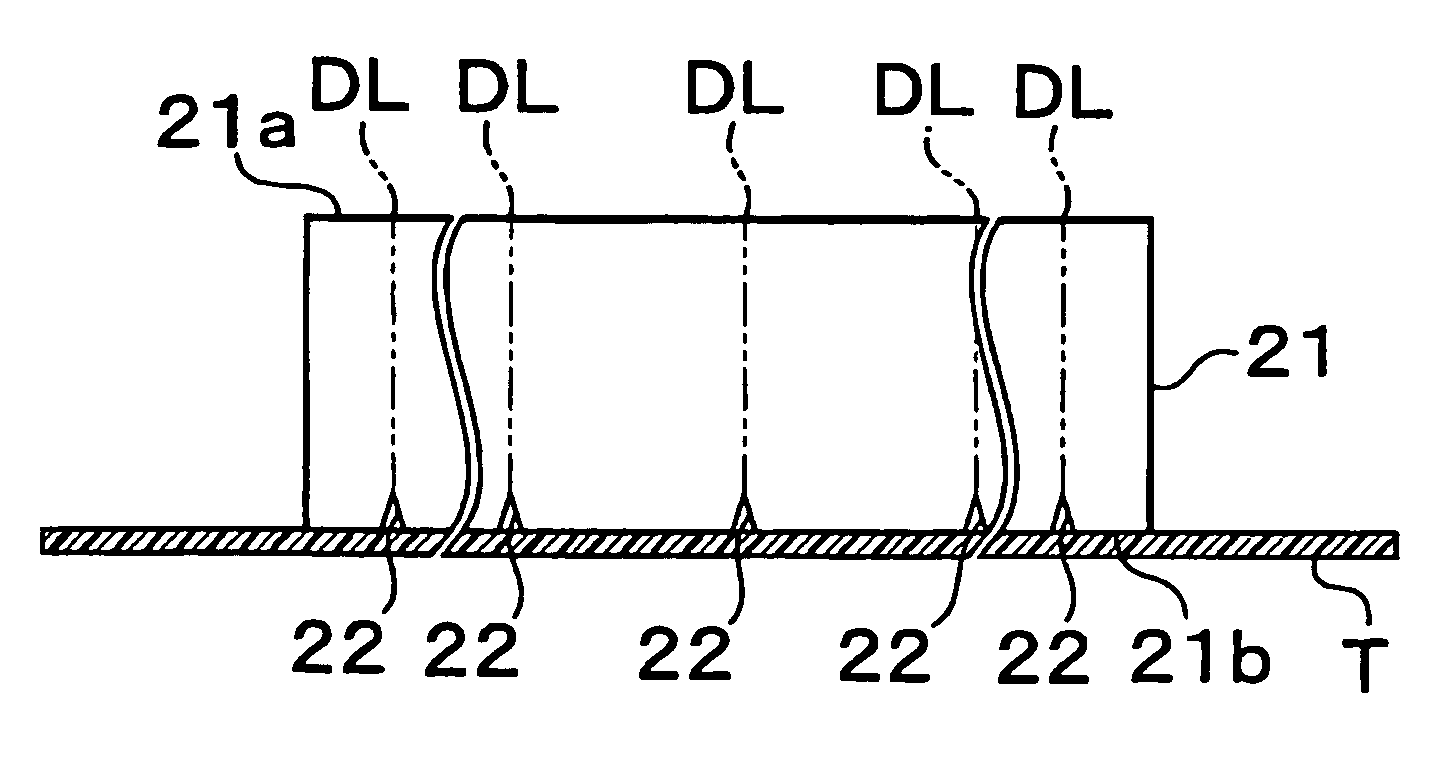
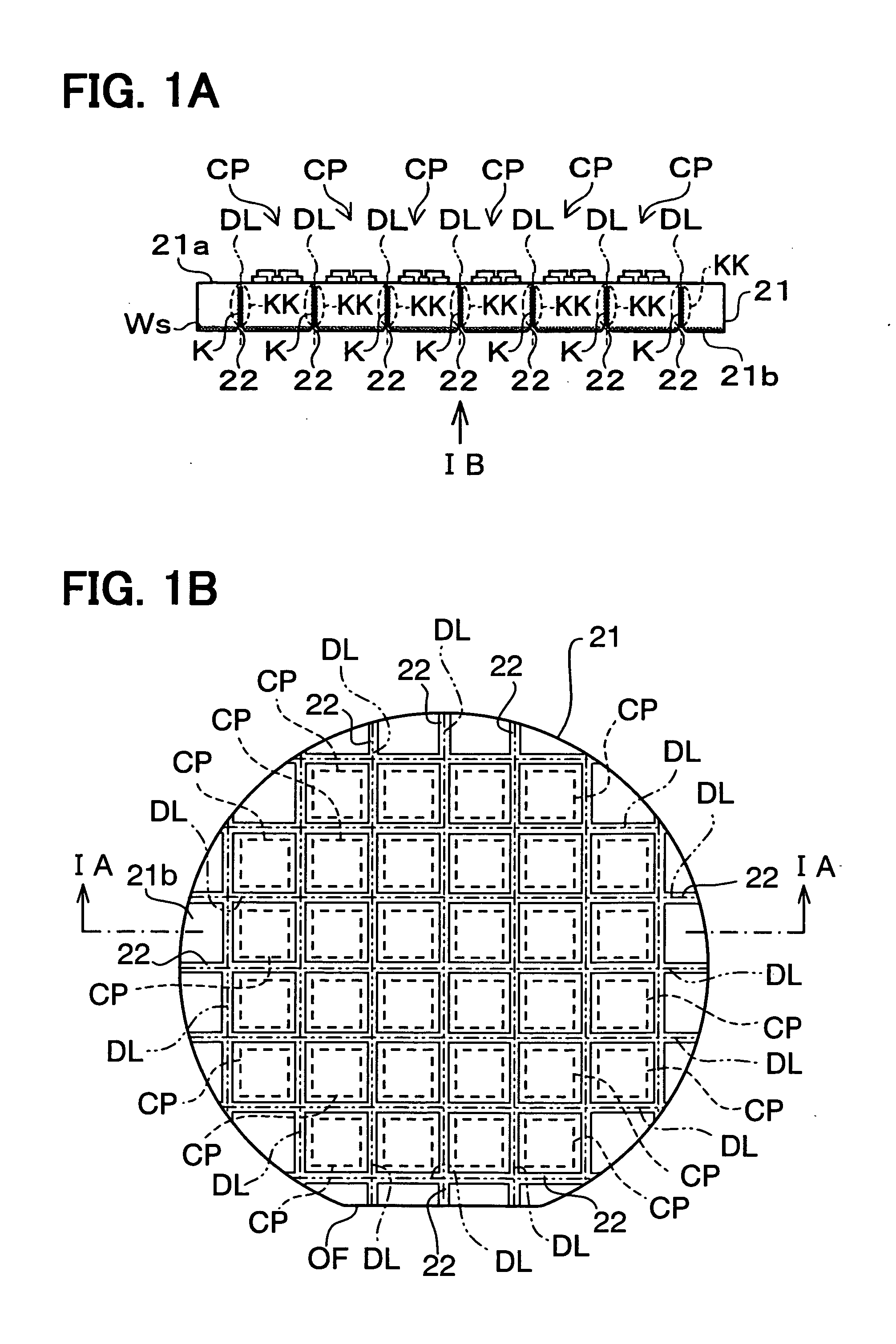
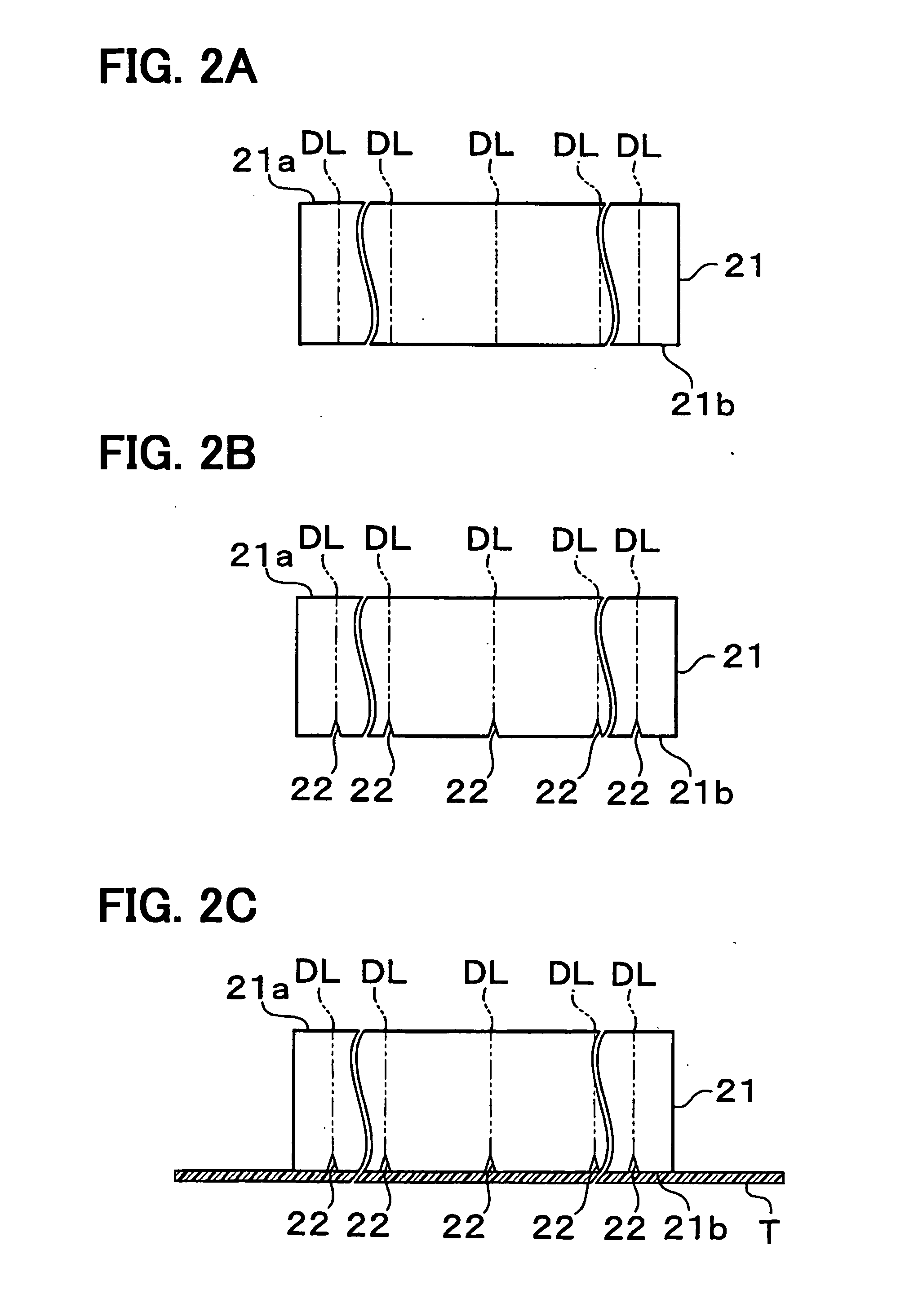
[0078] A laser dicing method and a semiconductor wafer in accordance with a first embodiment mode will be explained on the basis of FIGS. 1A to 3C. FIG. 1A illustrates a cross-sectional view (a section of line IA-IA shown in FIG. 1B) showing the construction of the semiconductor wafer in accordance with this first embodiment mode. FIG. 1B shows a bottom (rear) view seen from a line arrow IB shown in FIG. 1A. Further, FIGS. 2A to 3C illustrate cross-sectional views showing the construction of the semiconductor wafer in each step constituting a dicing process in accordance with this first embodiment mode. FIG. 2A shows the semiconductor wafer before a groove portion forming step. FIG. 2B shows the semiconductor wafer after the groove portion forming step. FIG. 2C shows the semiconductor w...

second embodiment

Mode

[0093] Next, a laser dicing method in accordance with a second embodiment mode will be explained on the basis of FIGS. 4A to 4C. FIGS. 4A to 4C illustrate cross-sectional views showing the construction of a semiconductor wafer in each step constituting a dicing process in accordance with this second embodiment mode. FIG. 4A shows the semiconductor wafer during the reforming layer forming step. FIG. 4B shows the semiconductor wafer after the groove portion forming step. FIG. 4C shows the semiconductor wafer after the expand tape sticking step.

[0094] This second embodiment mode differs from the first embodiment mode in that the groove portion forming step arranged before the reforming layer forming step in the first embodiment mode is arranged after the reforming layer forming step.

[0095] As shown in FIG. 4A, in this second embodiment mode, with respect to the semiconductor wafer 21 forming no groove portion 22 therein, a laser beam is first irradiated to the surface 21a of the ...

third embodiment

Mode

[0101] Next, a laser dicing method in accordance with a third embodiment mode will be explained on the basis of FIGS. 5A to 5D. FIGS. 5A to 5D illustrate cross-sectional views showing the construction of a semiconductor wafer in each step constituting a dicing process in accordance with this third embodiment mode. FIG. 5A shows the semiconductor wafer after the groove portion forming step. FIG. 5B shows the semiconductor wafer during the reforming layer forming step. FIG. 5C shows the semiconductor wafer seen from a line arrow VC shown in FIG. 5B. FIG. 5D shows the semiconductor wafer after the expand step.

[0102] This third embodiment mode differs from the first embodiment mode in that the groove portion 22 formed on the rear face 21b of the semiconductor wafer 21 in the first embodiment mode is formed as a groove portion 24 on the surface 21a of the semiconductor wafer 21. The groove portion 24 formed in this third embodiment mode differs from the groove portion 22 formed in t...


PUM

PropertyMeasurementUnit
Distanceaaaaaaaaaa
Thicknessaaaaaaaaaa
Forceaaaaaaaaaa

Abstract

A method for dicing a semiconductor substrate includes: forming a reforming layer in the substrate by irradiating a laser beam on the substrate; forming a groove on the substrate along with a cutting line; and applying a force to the substrate in order to cutting the substrate at the reforming layer as a starting point of cutting. The groove has a predetermined depth so that the groove is disposed near the reforming layer, and the force provides a stress at the groove.

Description

CROSS REFERENCE TO RELATED APPLICATIONS [0001] This application is based on Japanese Patent Applications No. 2005-331206 filed on Nov. 16, 2005, No. 2005-331219 filed on Nov. 16, 2005, No. 2005-331221 filed on Nov. 16, 2005, No. 2006-225394 filed on Aug. 22, 2006, No. 2006-225395 filed on Aug. 22, 2006, and No. 2006-271748 filed on Oct. 3, 2006, the disclosures of which are incorporated herein by reference. FIELD OF THE INVENTION [0002] The present invention relates to a semiconductor device and a dicing method for a semiconductor substrate. BACKGROUND OF THE INVENTION [0003] In a dicing process for cutting a processing object such as a silicon wafer, etc. forming a semiconductor integrated circuit and MEMS (Micro Electro Mechanical Systems), a dicing method using a dicing blade burying diamond grinding grains is formerly adopted. [0004] However, in the dicing method using such a blade, the following problems, etc. are caused. (1) When the processing object is cut by the blade, its ...

Claims


Application Information

Patent Timeline
IPC IPC(8): H01L21/00
CPCB23K26/0057B23K26/4075B23K2201/40B28D5/0011H01L21/78B23K26/40B23K26/53B23K2101/40B23K2103/50H01L21/30
Inventor KOMURA, ATSUSHITAMURA, MUNEOSUGIURA, KAZUHIKOFUNATO, HIROTSUGUMARUYAMA, YUMIFUJII, TETSUOKOHNO, KENJI
Owner DENSO CORP
Why Eureka
Try Eureka