

Selective etching of titanium nitride with xenon difluoride
a technology of xenon difluoride and selective etching, which is applied in the direction of coatings, chemical vapor deposition coatings, chemical apparatus and processes, etc., can solve the problems of inability to remove tin deposition products from semiconductor deposition chambers and equipment, and defective electronic product components
- Summary
- Abstract
- Description
- Claims
- Application Information
AI Technical Summary
Benefits of technology
Problems solved by technology
Method used
Image

Examples
example 1
Effectiveness of XeF2 in Etching of Deposition Materials at Various Temperatures and Pressures
[0034] In this example, the etch rates for TiN, SiO2, and SiN were determined using XeF2 as the etchant at various temperatures and pressures. Experimental samples were prepared from Si wafers coated with thin films of TiN, SiO2, and SiN. Etch rates were calculated by the thin film thickness change between the initial film thickness and that thickness after a timed exposure to the etching or processing conditions.
[0035] To effect etching bulk XeF2 gas was introduced from a cylinder into the reactor chamber through an unused remote plasma generator. The XeF2 gas pressure in the reactor chamber was held constant by turning off the flow from the cylinder once the desired pressure was reached.
[0036] The test coupons were placed on the surface of a pedestal heater which was used to maintain different substrate temperatures. The results are shown in Table 1 below.
TABLE 1ETCH RATES FOR VARIOU...
example 2
In Situ Formation of XeF2Via Reaction of Xe and NF3
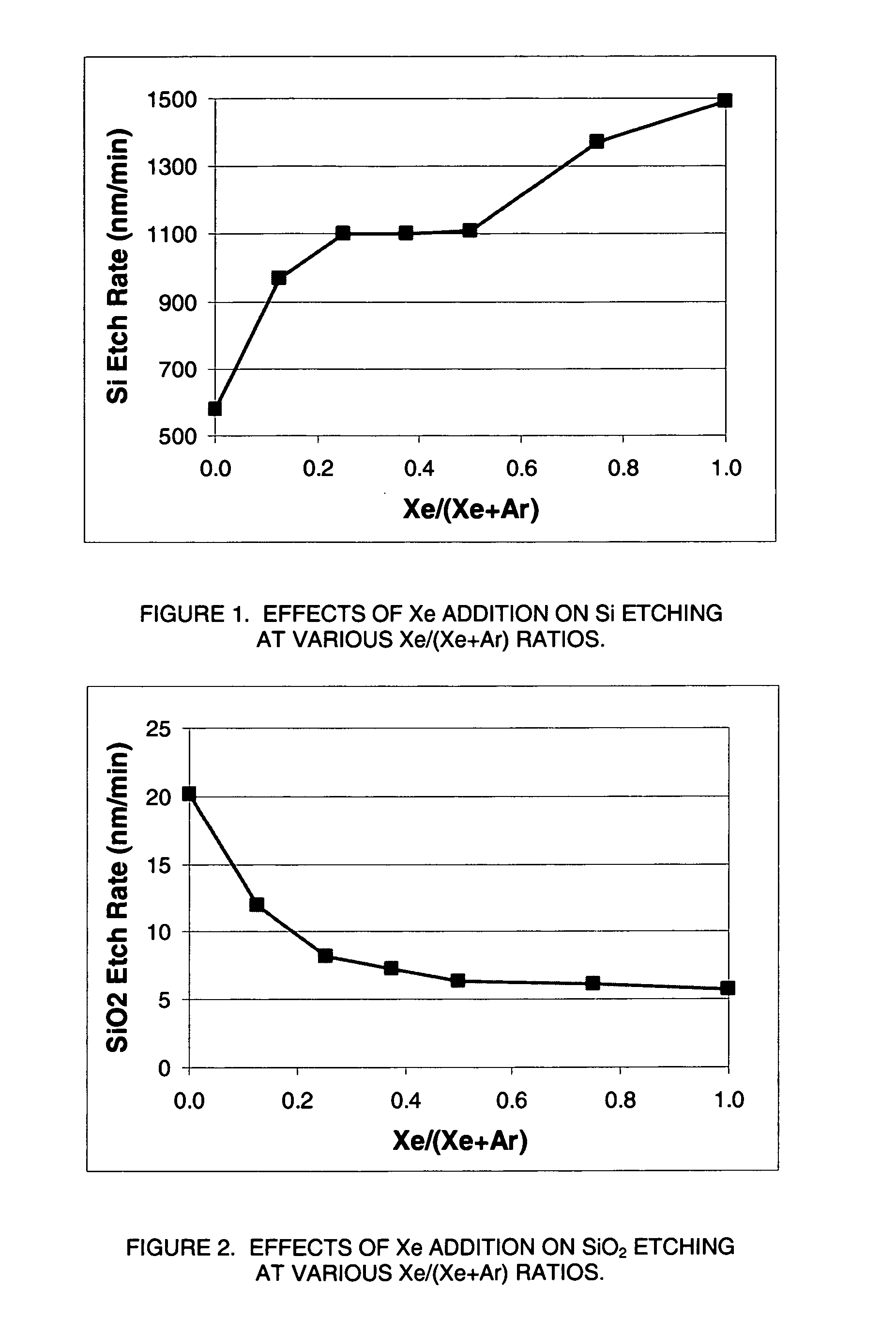
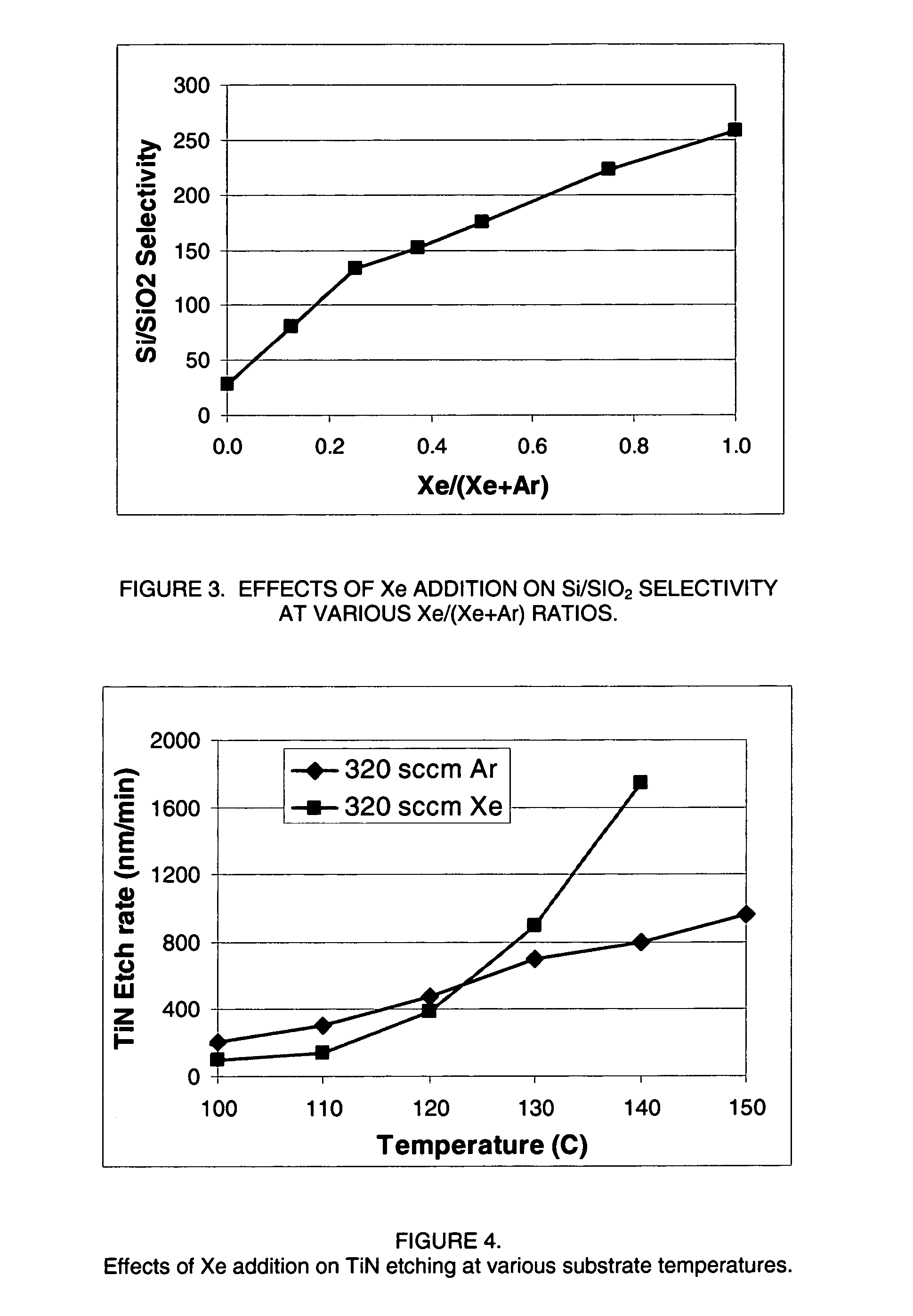
[0038] In this example, an MKS Astron remote plasma generator was mounted on top of a reactor chamber. The distance between the exit of the Astron generator and the sample coupon was about six inches. The remote plasma generator was turned on but the pedestal heater in the reactor chamber was turned off. The chamber was kept at room temperature. The etch rate of both Si and SiO2 substrates using remote plasma was measured for comparative purposes.
[0039] The process gas to the remote plasma was NF3 and it was mixed with a second gas stream in various amounts. The second gas stream was comprised of either Xe, argon (Ar), or a combination thereof. The total gas flowrate to the reactor chamber was fixed at 400 sccm and the NF3 flowrate was fixed at 80 sccm. While keeping the total flowrate of the second gas stream at 320 sccm, the ratio of the flowrate of Xe to the total flowrate of the second gas stream (Xe / (Ar+Xe)) was varied betwee...
example 3
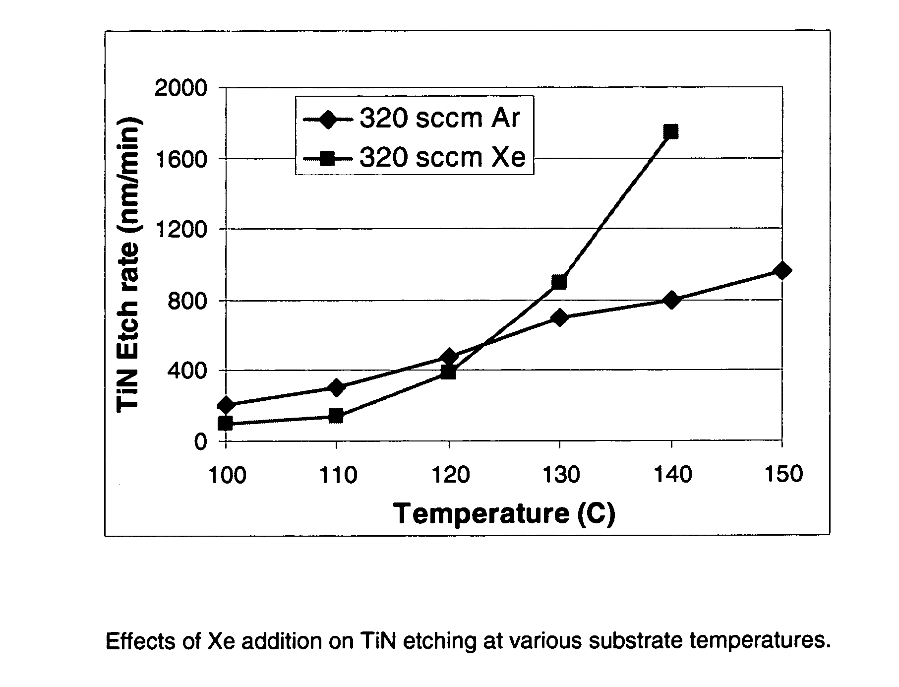
Effect of Remote Plasma and Temperature on Etch Rate of TiN and SiO2
[0043] In this example the procedure of Example 2 was followed except both the remote plasma generator and the pedestal heater were turned on to allow for determination of the etch rate of both TiN and SiO2 using remote plasma at various substrate temperatures.
[0044] In a first set of experiments the etch rate of TiN and SiO2 was measured using a mixture of NF3 and Xe as the process gas. The flowrate of Xe was fixed at 320 sccm. The temperature was varied from 100° C. to 150° C. The results of these experiments are shown as the square points in FIGS. 4 and 5 for TiN and SiO2, respectively.
[0045] In a second set of experiments the etch rate of TiN and SiO2 was measured using a mixture of NF3 and argon (Ar) as the process gas. The flowrate of Ar was fixed at 320 sccm. The temperature was varied from 100° C. to 150° C. The results of these experiments are shown as the diamond points in FIGS. 4 and 5 for TiN and SiO2...
PUM
| Property | Measurement | Unit |
|---|---|---|
| Temperature | aaaaa | aaaaa |
| Temperature | aaaaa | aaaaa |
| Temperature | aaaaa | aaaaa |
Abstract
Description
Claims
Application Information