Hetero-junction bipolar transistor

Inactive Publication Date: 2007-05-31
PANASONIC CORP
View PDF1 Cites 57 Cited by
  • Summary
  • Abstract
  • Description
  • Claims
  • Application Information

AI Technical Summary

Benefits of technology

[0072] As has been described, in each of the hetero-junction bipolar transistors (HBTs) according to the first through third aspects of the present invention, the delta-doped layer is provided in the first collector layer or the semiconductor layer or the spacer layer is provided

Problems solved by technology

That is, the larger the amount of electrons or holes is, the higher the possibility of occurrence of avalanche breakdown becomes.
That is, the higher the electric field intensity is, the higher the possibility of occurrence of avalanche breakdown becomes.
However, in the second known HBT, the following problems ari

Method used


Image

  • Hetero-junction bipolar transistor
  • Hetero-junction bipolar transistor
  • Hetero-junction bipolar transistor

Examples


first embodiment

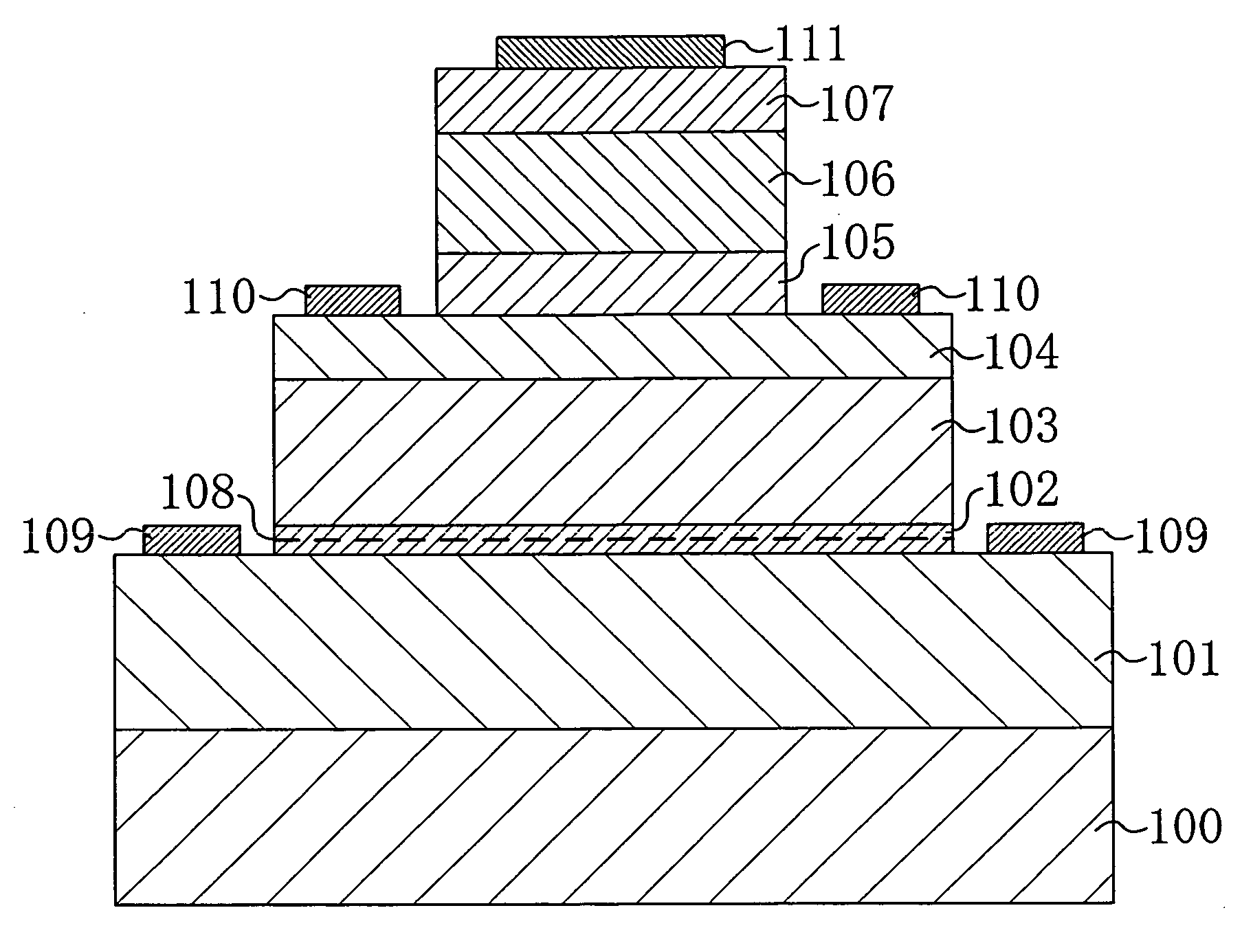
[0087] Hereafter, a structure of a HBT according to a first embodiment of the present invention will be described with reference to FIG. 1 and Table 1. FIG. 1 is a cross-sectional view illustrating the structure of the HBT according to the first embodiment of the present invention. Table 1 shows materials, conductivity types, film thicknesses, carrier concentrations and sheet concentrations for a substrate and each semiconductor layer in the HBT according to the first embodiment of the present invention.

[0088] An object of this embodiment is to realize a HBT having a low on-state resistance and a high breakdown voltage when the HBT is in a high output operation.

[0089] As shown in FIG. 1, a sub-collector layer 101, a first collector layer 102 including a delta-doped layer 108 therein, a second collector layer 103, a base layer 104, a first emitter layer 105, a second emitter layer 106 and an emitter contact layer 107 are formed in this order on a substrate 100 by MOCVD (metal organ...

second embodiment

[0107] Hereafter, a structure of a HBT according to a second embodiment of the present invention will be described with reference to FIG. 4 and Table 2. FIG. 4 is a cross-sectional view illustrating the structure of the HBT according to the second embodiment of the present invention. Table 2 shows materials, conductive types, film thicknesses and carrier concentrations for a substrate and each semiconductor layer in the HBT according to the second embodiment of the present invention.

[0108] An object of this embodiment is the same as that of the first embodiment, i.e., to realize a HBT having a low on-state resistance and a high breakdown voltage when the HBT is in a high output operation.

[0109] As shown in FIG. 4, a sub-collector layer 201, a first collector layer 202, a composition-graded layer 208, a second collector layer 203, a base layer 204, a first emitter layer 205, a second emitter layer 206 and an emitter contact layer 207 are formed in this order on a substrate 200 by M...

third embodiment

[0124] Hereafter, a structure of a HBT according to a third embodiment of the present invention will be descried with reference to FIG. 6 and Table 3. FIG. 6 is a cross-sectional view illustrating the structure of the HBT according to the third embodiment of the present invention. Table 3 shows materials, conductive types, film thicknesses and carrier concentrations for a substrate and each semiconductor layer in the HBT according to the third embodiment of the present invention.

[0125] An object of this embodiment is the same as those of the first and second embodiments, i.e., to realize a HBT having a low on-state resistance and a high breakdown voltage when the HBT is in a high output operation.

[0126] As shown in FIG. 6, a sub-collector layer 301, a first collector layer 302, a spacer layer 308, a second collector layer 303, a base layer 304, a first emitter layer 305, a second emitter layer 306 and an emitter contact layer 307 are formed in this order on a substrate 300 by MOCV...


PUM


Abstract

A hetero-junction bipolar transistor includes a sub-collector layer formed on a substrate and having conductivity, a first collector layer formed on the sub-collector layer and a second collector layer formed on the first collector layer and having the same conductive type as a conductive type of the sub-collector layer. In the first collector layer, a delta-doped layer is provided.

Description

CROSS-REFERENCE TO RELATED APPLICATION [0001] The disclosure of Japanese Patent Applications No. 2005-293774 filed on Oct. 6, 2005 including specification, drawings and claims are incorporated herein by reference in its entirety. BACKGROUND OF THE INVENTION [0002] The present invention relates to hetero-junction bipolar transistors. [0003] Compound semiconductor devices such as a field-effect transistor (which will be hereafter referred to as a “FET”) or a hetero-junction bipolar transistor (HBT) are used for, for example, transmitting high output power amplifiers which are of a cellular phone component, and the like. In recent years, high output power characteristics, high gain characteristics and low distortion characteristics have been required for HBTs. To achieve those characteristics, the development of a high breakdown voltage and low on-state resistant HBT has been demanded. [0004] Hereafter, a structure of a known HBT will be described with reference to FIG. 8 and Table 4. ...

Claims


Application Information

Patent Timeline
IPC IPC(8): H01L31/00H01L29/739
CPCH01L29/0821H01L29/7371
Inventor NOGOME, MASANOBU
Owner PANASONIC CORP
Why Eureka
Try Eureka