

Plasma display panel
a technology of display panel and plasma, which is applied in the manufacture of discharge tube/lamp, discharge tube coating, electrode system manufacturing, etc., can solve the problems of black noise, electron beam plating process, hard to maintain display quality within a certain level, etc., and achieve the effect of improving the quality of the display
- Summary
- Abstract
- Description
- Claims
- Application Information
AI Technical Summary
Benefits of technology
Problems solved by technology
Method used
Image

Examples
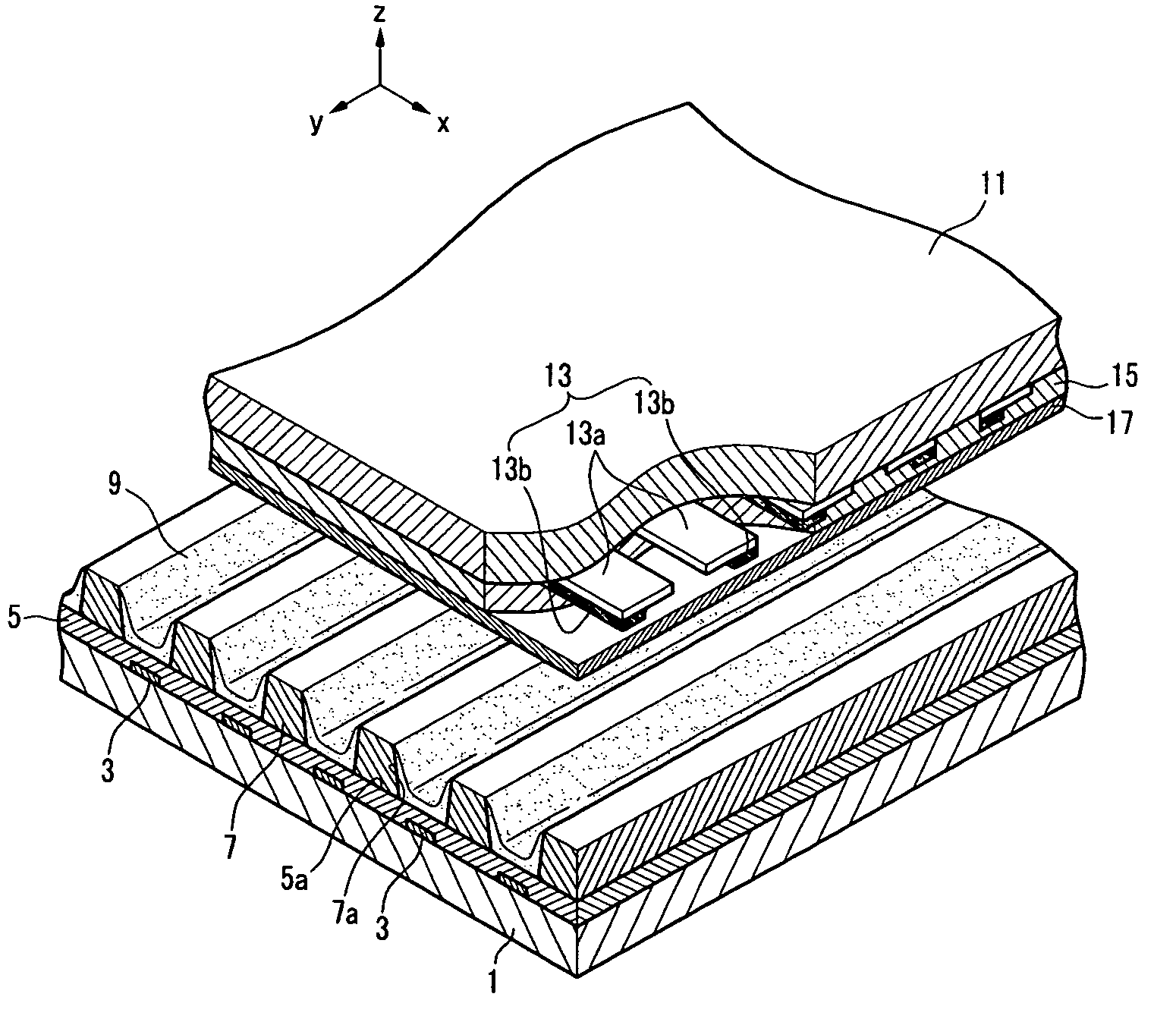
example 1
[0042] On an upper substrate of soda lime glass, display electrodes were formed into a stripe shape using an indium tin oxide conductive material in accordance with the generally used method in this art.
[0043] Subsequently, a lead-based glass paste was coated on the entire surface of the upper substrate while covering display electrodes and fired to provide a second dielectric layer.
[0044] Fused MgO was ion-plated on the second dielectric layer to provide a MgO protective layer.
experimental example 1
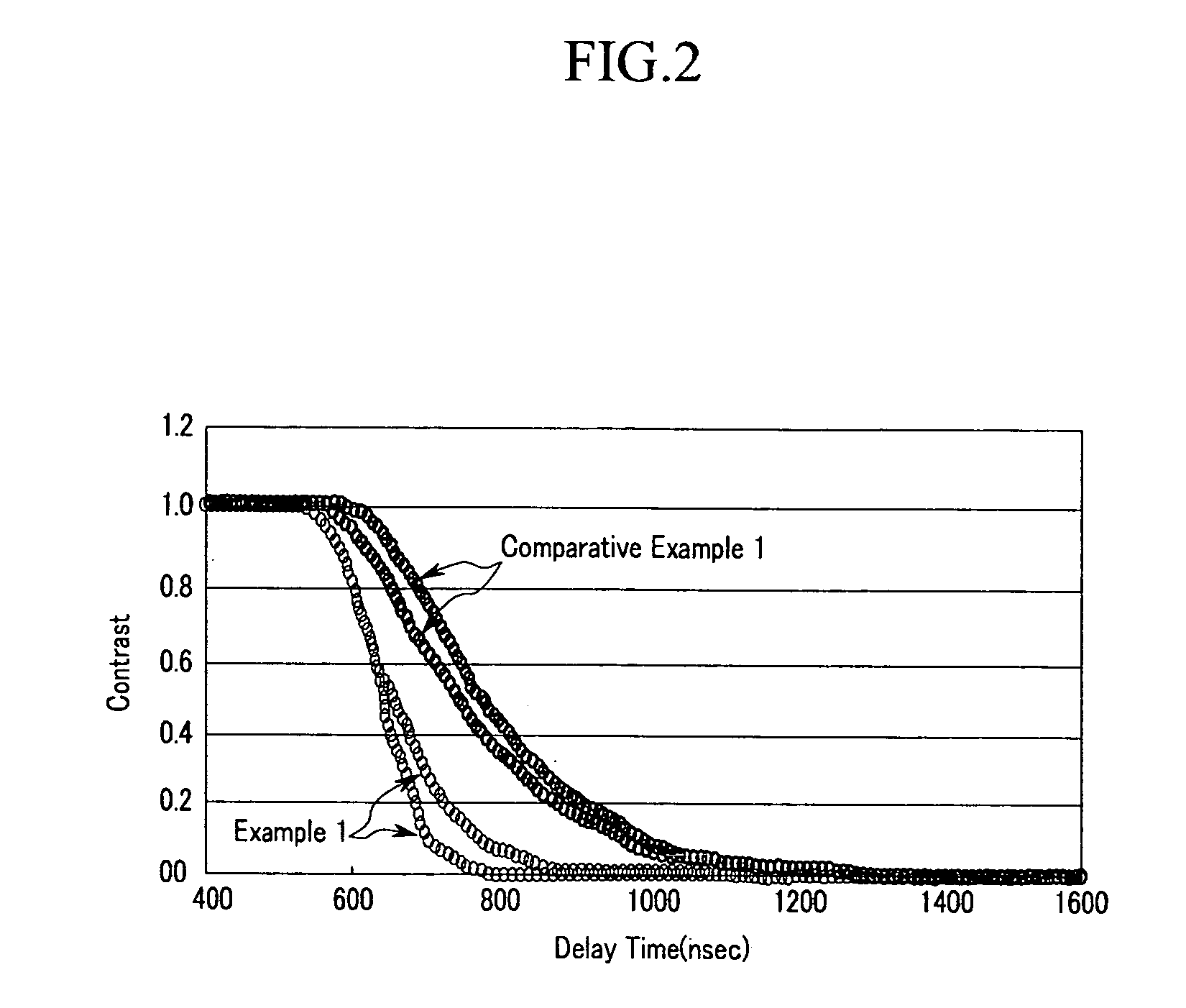
Comparison of Response speed depending upon Deposition Process
[0047] To compare the difference between the ion-plating and the electron beam plating, the protective layers according to Example 1 and Comparative Example 1 were measured two times to determine the response speed, and the results are shown in FIG. 2. The response speed is determined when the white level (contrast 1.0) is changed to the black level (contrast 0.0) by applying a voltage. A delayed response speed may cause an after image when an image is continuously displayed.
[0048] Referring to FIG. 2, the protective layer prepared by the ion-plating in accordance with Example 1 has a shorter delay time than that of the electron beam plating in accordance with Comparative Example 2. From the results, it can be seen that the response speed was improved due to the ion-plating.
experimental example 2
Comparison of Crystalline Grain Diameter
[0049] To compare the crystalline grain diameters of the protective layers prepared by the ion-plating and the electron beam plating, the surfaces of the protective layers according to Example 1 and Comparative Example 1 were observed by a scanning electron microscope. The obtained results are shown in FIG. 3A (Example 1) and FIG. 3B (Comparative Example 1).
[0050] Referring to FIG. 3A, the MgO protective layer prepared by the ion-plating in accordance with Example 1 was composed of single-crystalline MgO with a crystalline grain diameter ranging from about 100 to 200 nm, and a membrane density thereof was 3.0 g / cm3. The refractive index at 650 nm of the MgO protective layer was 1.64.
[0051] The MgO protective layer prepared by the electron beam plating in accordance with Comparative Example 1 had a refractive index at 650 nm of 1.62. From the results, it shows that it was composed of single-crystalline MgO. However, the crystalline grain dia...
PUM
 Abstract
Description
Claims
Application Information