
Methods for Producing Diode-Pumped Micro Lasers

a technology of diode pumping and lasers, applied in lasers, semiconductor lasers, active medium materials, etc., can solve the problem achieve the effect of low unit cost, high beam quality and good reliability

Inactive Publication Date: 2007-05-31
SNAKE CREEK LASERS
View PDF52 Cites 34 Cited by
  • Summary
  • Abstract
  • Description
  • Claims
  • Application Information

AI Technical Summary

Benefits of technology

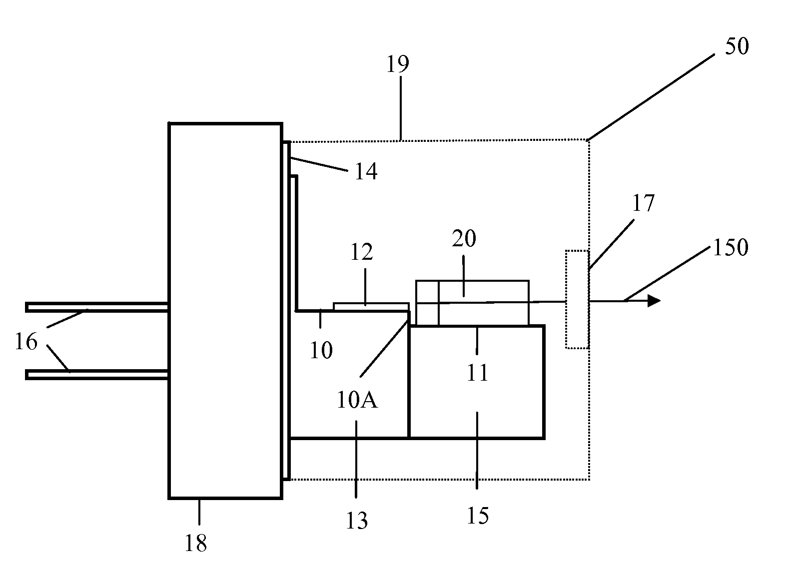
[0016] A miniaturized laser package includes a modern laser diode package (LDP), modified to accept a solid state microchip assembly pumped by the diode laser. The microchip assembly is added to standard LDPs containing laser diodes mounted on heatsinking shelves by affixing a second shelf to mount and heatsink the microchip assembly. Standard packages described in the invention include 9 mm and 5.6 mm packages, all of which are characterized by small dimensions, well sealed housing, robust mounting features, known characterized materials, and economical production and assembly techniques characteristic of the laser diode industry. In particular, the microchip lasers are produced using techniques that lend themselves to mass production, resulting in very low unit costs. The compact laser devices provide laser radiation at high beam quality and good reliability with a variety of wavelengths and operational characteristics and low noise features not available in prior art diode lasers, while relying primarily on standardized designs, materials, and techniques common to diode laser manufacturing. The devices constructed according to methods taught by the present invention can therefore be readily integrated into numerous applications where power, reliability, and performance are at a premium but low cost is essential, eventually replacing diode lasers in many existing systems and also enabling many new commercial, biomedical, scientific, and military systems.
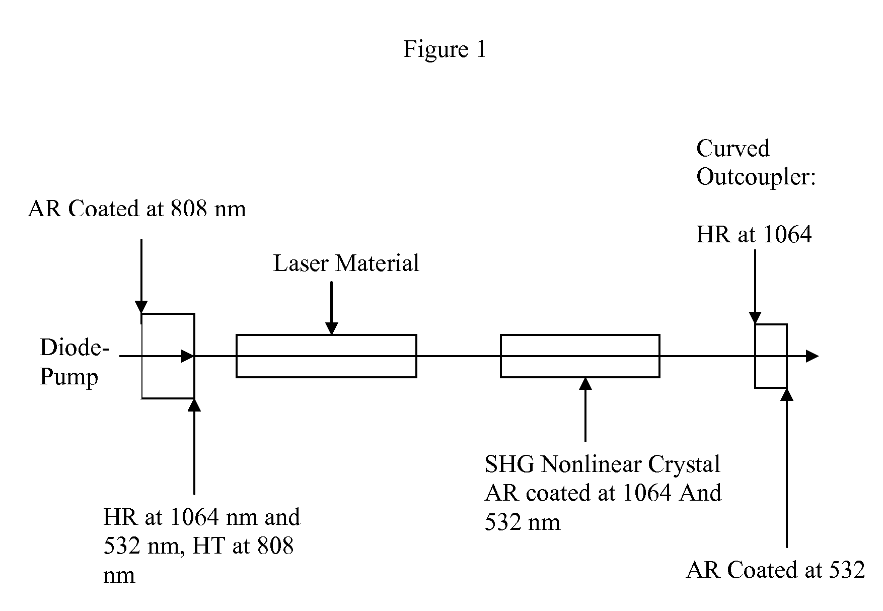
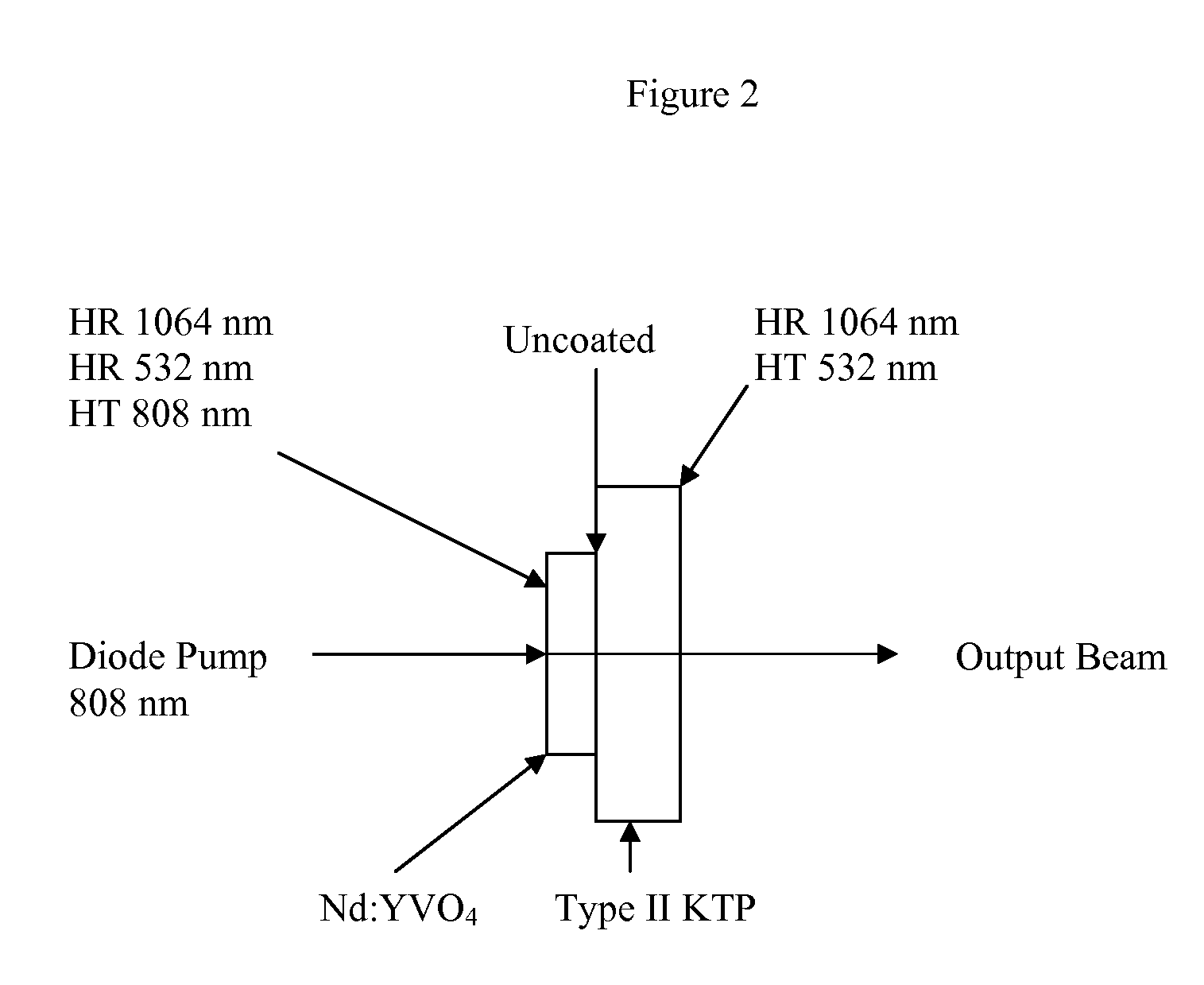
[0017] This invention addresses methods for producing high-density low-cost micro and miniature laser resonators with high beam quality laser radiation that can be assembled in highly compact packages using fabrication methodologies compatible with mass production and low unit costs (<$25). The present invention provides solutions to the challenge of designing for manufacturability using techniques characterized by their simplicity, cost effectiveness, and adaptability to operation at many different modes and a variety of wavelengths in either the visible or beyond. The invention further emphasizes those packaging technologies, laser designs, and materials that can provide high performance without compromising reliability of the microlaser devices, all at a material cost that can be as low as one to a few dollars. This makes the miniature devices of the present invention suitable to be integrated into numerous applications including the consumer and biomedical markets, potentially supplanting and replacing existing diode laser technology. The techniques disclosed also lend themselves to microlasers that can produce radiation at a large variety of operational modes and wavelengths. Specifically, the present invention provides improved methods, systems, and devices for providing cost effectively operational modes that include SLM in both CW and pulsed versions and spectral ranges that extend into the eye-safe region on one end and the UV region on the other end.

Problems solved by technology

In particular, the microchip lasers are produced using techniques that lend themselves to mass production, resulting in very low unit costs.

Method used


Image

  • Methods for Producing Diode-Pumped Micro Lasers
  • Methods for Producing Diode-Pumped Micro Lasers
  • Methods for Producing Diode-Pumped Micro Lasers

Examples


Embodiment Construction

[0038] The present invention includes solid-state laser crystals incorporated into laser diode packages like the 5.6 mm and 9 mm, which already include a diode laser. In contrast, U.S. Pat. No. 6,891,879, to Peterson, uses a large TO-3 package to construct diode-pumped solid-state lasers that are extra-cavity doubled. In addition, unlike the present invention which relies on modern laser diode packages (LDPs), Peterson utilizes an older TO-3 package in which the diode and the crystals and alignment features must be mounted. The present invention is very different from Peterson, because green lasers of the present invention easily replace red diode lasers using modern laser diode packages, because the package diameter is the same and so are the electrical connections. Thus, unlike the devices in Peterson, the green lasers of the present invention may be plugged into spaces and receptacles previously used for red diode lasers.

[0039] The laser diode packages of the present invention a...


PUM


Abstract

A miniaturized laser package includes a modern LDP, modified to accept a solid state microchip assembly pumped by the diode laser. The microchip assembly is added to standard LDPs containing laser diodes mounted on heatsinking shelves by affixing a second shelf to mount and heatsink the microchip assembly. Standard packages described in the invention include 9 mm and 5.6 mm packages, all of which are characterized by small dimensions, well sealed housing, robust mounting features, known characterized materials, economical production, and assembly techniques characteristic of the semiconductor processing industry.

Description

REFERENCE TO RELATED APPLICATIONS [0001] This is a continuation in part application of co-pending application Ser. No. 10 / 946,941, filed Sep. 22, 2004, entitled “HIGH DENSITY METHODS FOR PRODUCING DIODE-PUMPED MICRO LASERS”, which claimed an invention which was disclosed in Provisional Application No. 60 / 504,617, filed Sep. 22, 2003, entitled “HIGH DENSITY METHODS FOR PRODUCING DIODE-PUMPED MICRO LASERS”. The benefit under 35 USC §119(e) of the United States provisional application is hereby claimed, and the aforementioned applications are hereby incorporated herein by reference.BACKGROUND OF THE INVENTION [0002] 1. Field of the Invention [0003] The present invention relates to highly compact and / or miniaturized diode pumped solid state lasers that are fabricated using industry standard laser diode packages. [0004] 2. Description of Related Art [0005] New types of microlasers are desired as a replacement for conventional red lasers, particularly red semiconductor diode lasers that a...

Claims


Application Information

Patent Timeline
IPC IPC(8): H01S3/14H01S3/02H01S3/04H01S3/06H01S3/07H01S3/091H01S3/0941H01S3/108H01S3/131H01S3/16H01S5/00
CPCH01S3/025H01S3/0405H01S3/0604H01S3/0627H01S3/09415H01S3/109H01S3/113H01S3/1317H01S3/1611H01S3/1673
Inventor BROWN, DAVID C.
Owner SNAKE CREEK LASERS
Learn More