Method of nanopatterning, a resist film for use therein, and an article including the resist film

a resist film and nano-patterning technology, applied in nanoinformatics, photomechanical devices, instruments, etc., can solve the problems of high adhesive force between a mold surface and the resist film, fracture and/or delamination of the resist film from the substrate, and poor pattern transfer of the large aspect ratio structure, etc., to achieve excellent resistance to oxygen plasma etching, low surface energy, and easy mold release

Inactive Publication Date: 2007-05-31
DOW CORNING CORP
View PDF10 Cites 63 Cited by
  • Summary
  • Abstract
  • Description
  • Claims
  • Application Information

AI Technical Summary

Benefits of technology

[0009] The organosilicone-organic copolymer provides many advantages. For example, the copolymer is sufficiently elastic, due to the presence of the organosilicone component, to be capable of resisting fracture and delamination during mold release from a surface of a mold. Furthermore, the copolymer develops relatively low surface energy at an interface with

Problems solved by technology

When the conventional polymeric materials are used, high adhesive forces arise between a surface of the mold and the resist film due to a relatively large contact area between the surface of the mold and the resist film.
The high adhesive forces often result in fracture and/or delamination of the resist film from the substrate during mold release.
Furthermore, the high adhesive forces make forming large aspec

Method used


Image

  • Method of nanopatterning, a resist film for use therein, and an article including the resist film
  • Method of nanopatterning, a resist film for use therein, and an article including the resist film
  • Method of nanopatterning, a resist film for use therein, and an article including the resist film

Examples


example 1

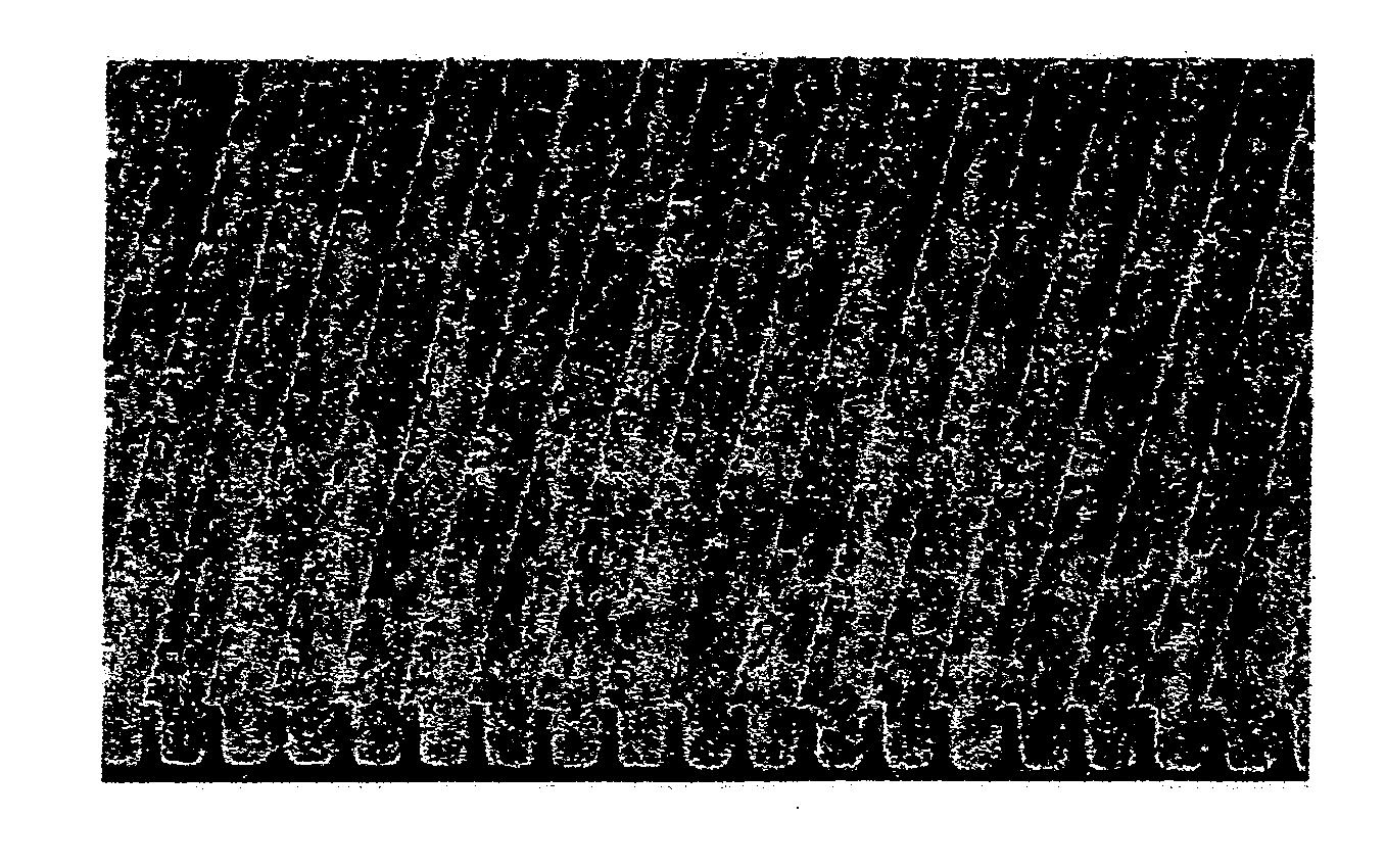
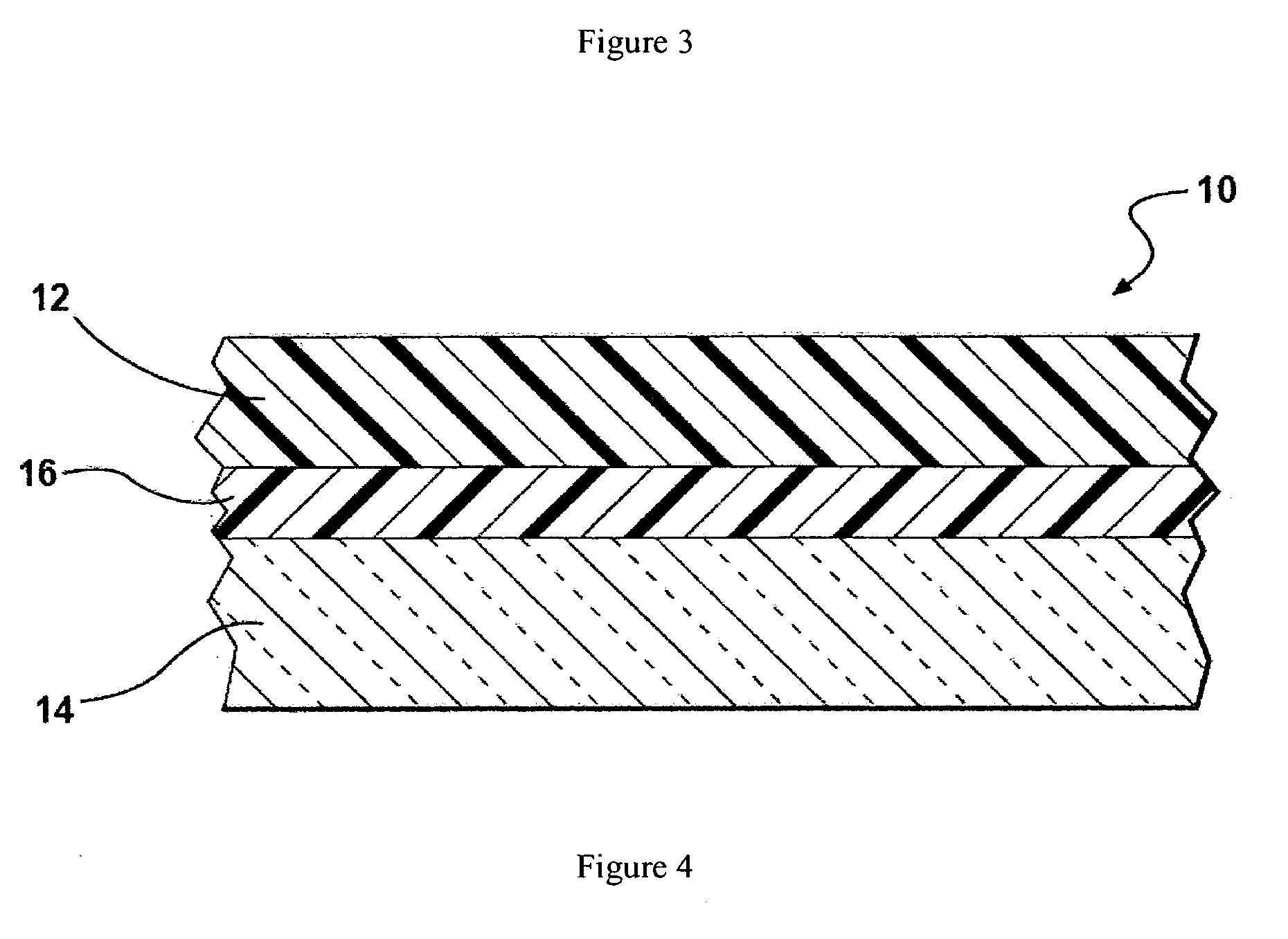
[0035] A planarizing film 16 including PMMA is first formed on a silicon substrate 14. More specifically, the PMMA is dissolved in toluene to form a planarizing solution, which is spin-coated onto the silicon substrate 14 to form the planarizing film 16. The planarizing film 16 has a thickness of about 400 nm. A Polystyrene-poly(dimethyl siloxane) diblock copolymer containing approximately 50% of PS and 50% of PDMS by weight (GPC: Mn=45,000 g / mol; Mw / Mn=1.10) is dissolved in PGMEA. The copolymer, i.e., the solution of the copolymer, is spin-coated onto the planarizing film 16 to form a resist film 12 having a thickness of about 300 nm. A nano- and micron-scale pattern is formed in the resist layer using a NX-1000 imprinter commercially available from Nanonex, Inc. of Monmouth Junction, N.J. A scanning electron microscopy (SEM) micrograph of the pattern is illustrated in FIG. 1.

example 2

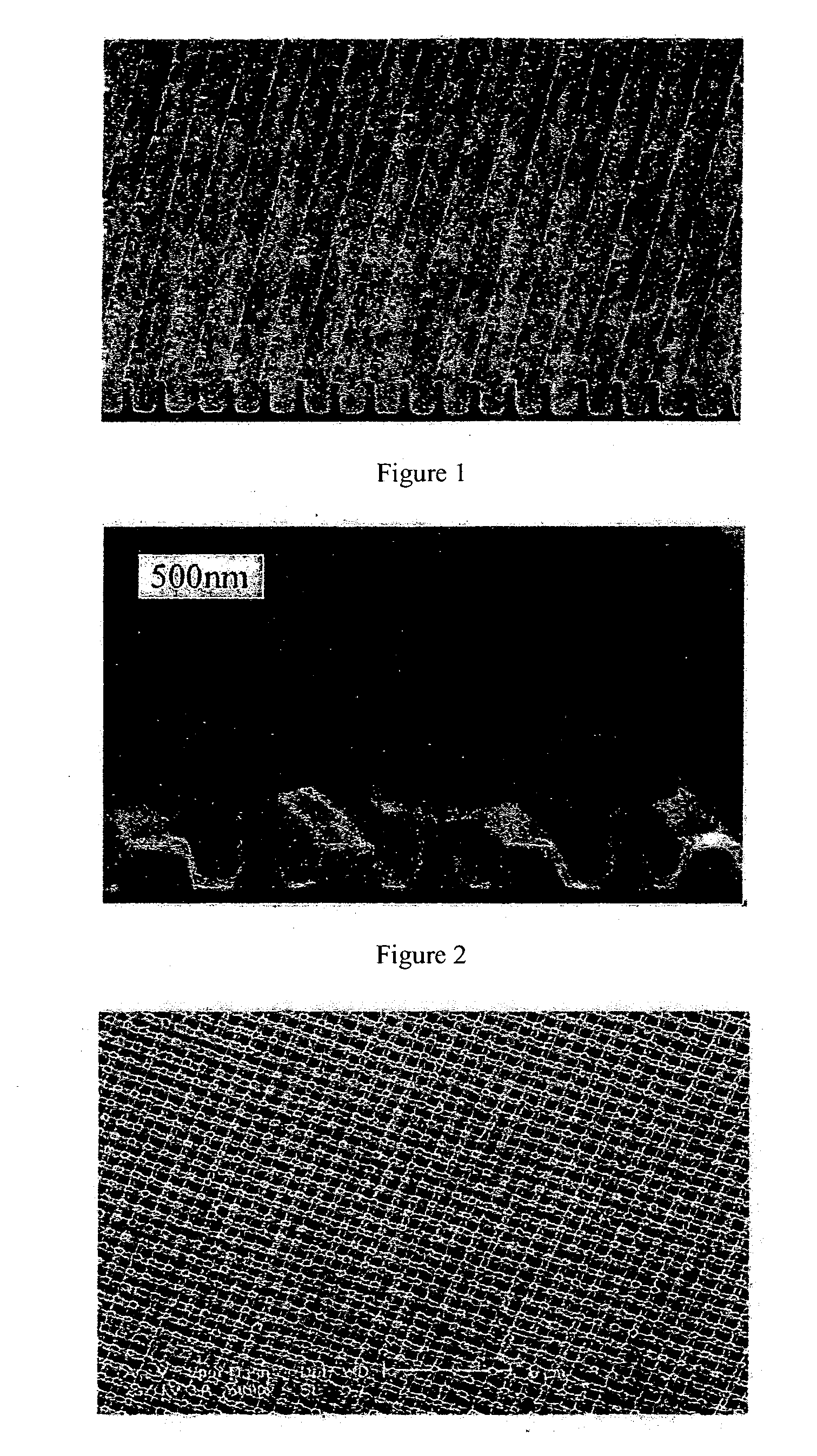
[0036] The planarizing film 16 and the resist film 12 are formed on the substrate 14 as described above in Example 1. However, the patterns are formed through imprinting so as not to completely extend through the resist film 12 into the planarizing film 16. After imprinting, the mold and the substrate 14 are separated and a replica of the mold pattern is imprinted into the resist film 12 (see, for example, FIG. 1).

[0037] Residual copolymer in the pattern is removed through fluorine plasma etching to expose the planarizing film 16. A lift-off process is then carried out by oxygen plasma etching the resist film 12 and the planarizing film 16. The oxygen plasma etch rate of the copolymer is about 0.98 nm / min., and the oxygen plasma etch rate of the PMMA is about 110 nm / min. As a result of this disparity in oxygen plasma etch rates, the undercut feature is achieved, as illustrated in FIG. 2. Due to the presence of silicon in the resist film 12, the resist film 12 shows very interesting...


PUM


Abstract

A method of nanopatterning includes the steps of providing a resist film (12) and forming a pattern in the resist film (12). The resist film (12) includes a copolymer consisting of an organosilicone component and an organic component. An article (10) includes a substrate (14) and the resist film (12) disposed on the substrate (14). The copolymer of the organosilicone component and the organic component is sufficiently elastic, due to the presence of the organosilicone component, to be capable of resisting fracture and delamination during mold release. Furthermore, during pattern formation, the copolymer develops relatively low surface energy at an interface with the surface of a mold, as compared to conventional polymeric materials, and preferentially adheres to the substrate (14) rather than the mold, which provides for relatively easy mold release. The presence of the organosilicone component in the copolymer also allows the resist film (12) to exhibit excellent resistance to oxygen plasma etching.

Description

GOVERNMENT LICENSE RIGHTS [0001] The U.S. Government has a paid-up license in this invention and the right in limited circumstances to require the patent owner to license others on reason-able terms as provided for by the terms of grant number ECF 0424204 awarded by the National Science Foundation.FIELD OF THE INVENTION [0002] The present invention generally relates to a method of nanopatterning, a resist film having a pattern formed therein, and an article including the resist film. More specifically, the resist film includes a copolymer that provides many advantages over conventional polymeric materials used in resist films for nanopatterning. BACKGROUND OF THE INVENTION [0003] Nanopatterning is an essential part of nanotechnology research for fabricating nanostructures. For these nanostructures and nanopatterning techniques to have significant practical value, low cost and high throughput nanopatterning techniques are indispensable. Among many new emerging techniques that are aim...

Claims


Application Information

Patent Timeline
IPC IPC(8): G03C5/00
CPCB82Y10/00B82Y40/00G03F7/0002G03F7/0757
Inventor FU, PENG FEIGUO, LINGJIE JAY
Owner DOW CORNING CORP
Why Eureka
Try Eureka