Printed wiring board and method for manufacturing the same

Inactive Publication Date: 2007-06-07
SAMSUNG ELECTRO MECHANICS CO LTD
View PDF2 Cites 259 Cited by
  • Summary
  • Abstract
  • Description
  • Claims
  • Application Information

AI Technical Summary

Benefits of technology

[0025] In order to fully harden the insulating layer and firing the conductive layer, the thermal treatment may be performed at 200-400° C., more preferably 200-350° C. In the printed wiring board of the present invention, the sem

Problems solved by technology

The subtractive process, however, is complex and presents a problem of having to dispose of waste liquid during the plating process or the etching process.
The above-described conventional methods have a problem in that the peel strength between the insulatin

Method used


Image

  • Printed wiring board and method for manufacturing the same
  • Printed wiring board and method for manufacturing the same
  • Printed wiring board and method for manufacturing the same

Examples


embodiment 1

[0075] Silver nitride and PVP (MW=10,000) were mixed at a mole ratio of 1:8, and dimethyl formamide (DMF) was added as a reducing agent to a purified water at a volume ratio of 1:1. Then, the reaction was conducted at 100° C. for 30 minutes. Consequently, the conductive ink with 50-nm silver nano particles caped with PVP was prepared.

[0076] The insulating ink was prepared by mixing polyimide precursor, photo-polymerization initiator, and crosslinking agent, as shown in Table 1 below. In Table 1, PAA represents polyamic acid that is the polyimide precursor, MBHP (4,4′-methylenebis[2,6-bis(hydroxymthyl)]phenol) was used as the crosslinking agent. PTMA(5-propylsulfonly-oxyimino-5H-thiophen-2-ylidene)-2-(methylphenyl)-acetonitrile) was used as the photo-polymerization initiator.

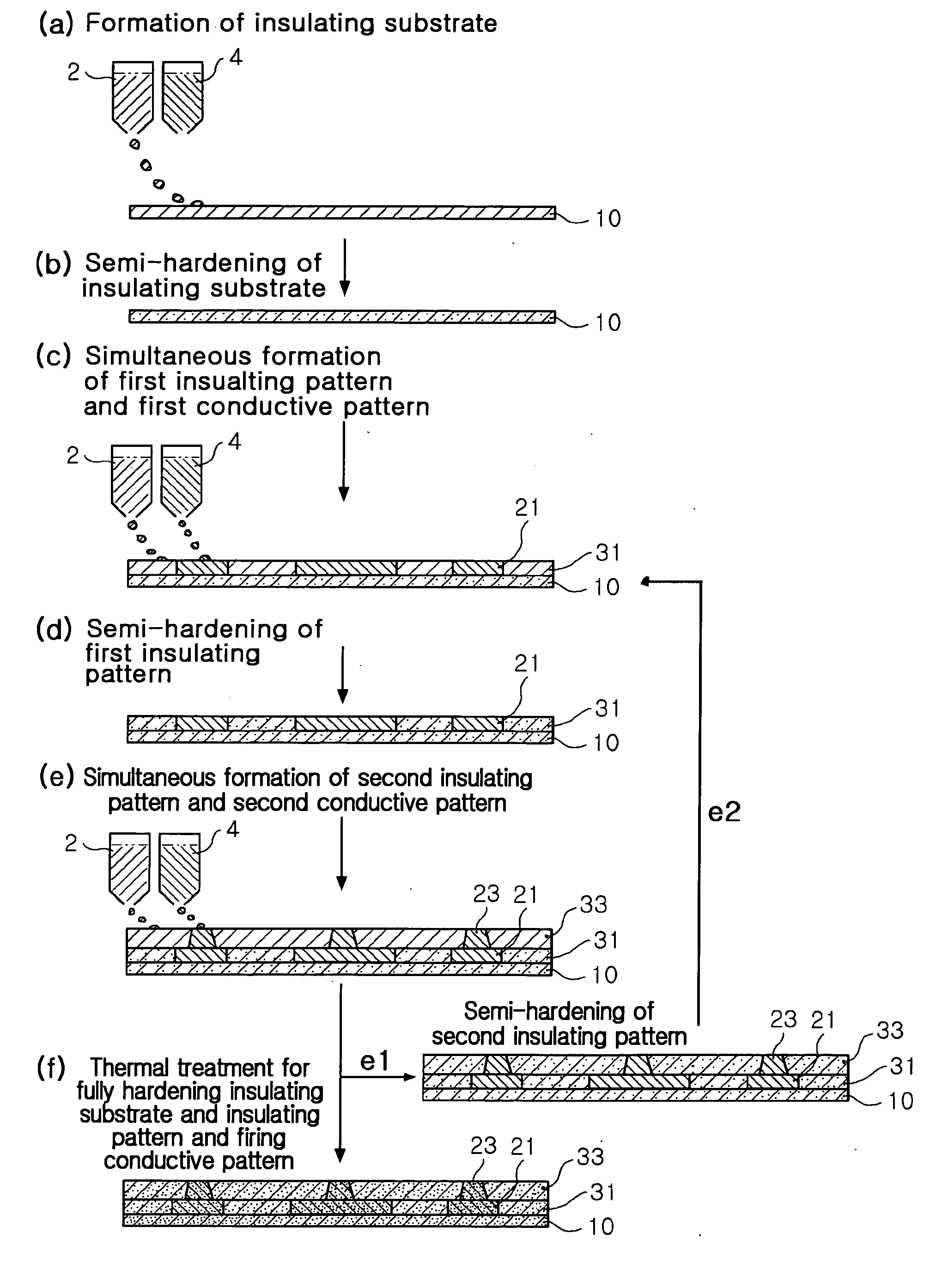
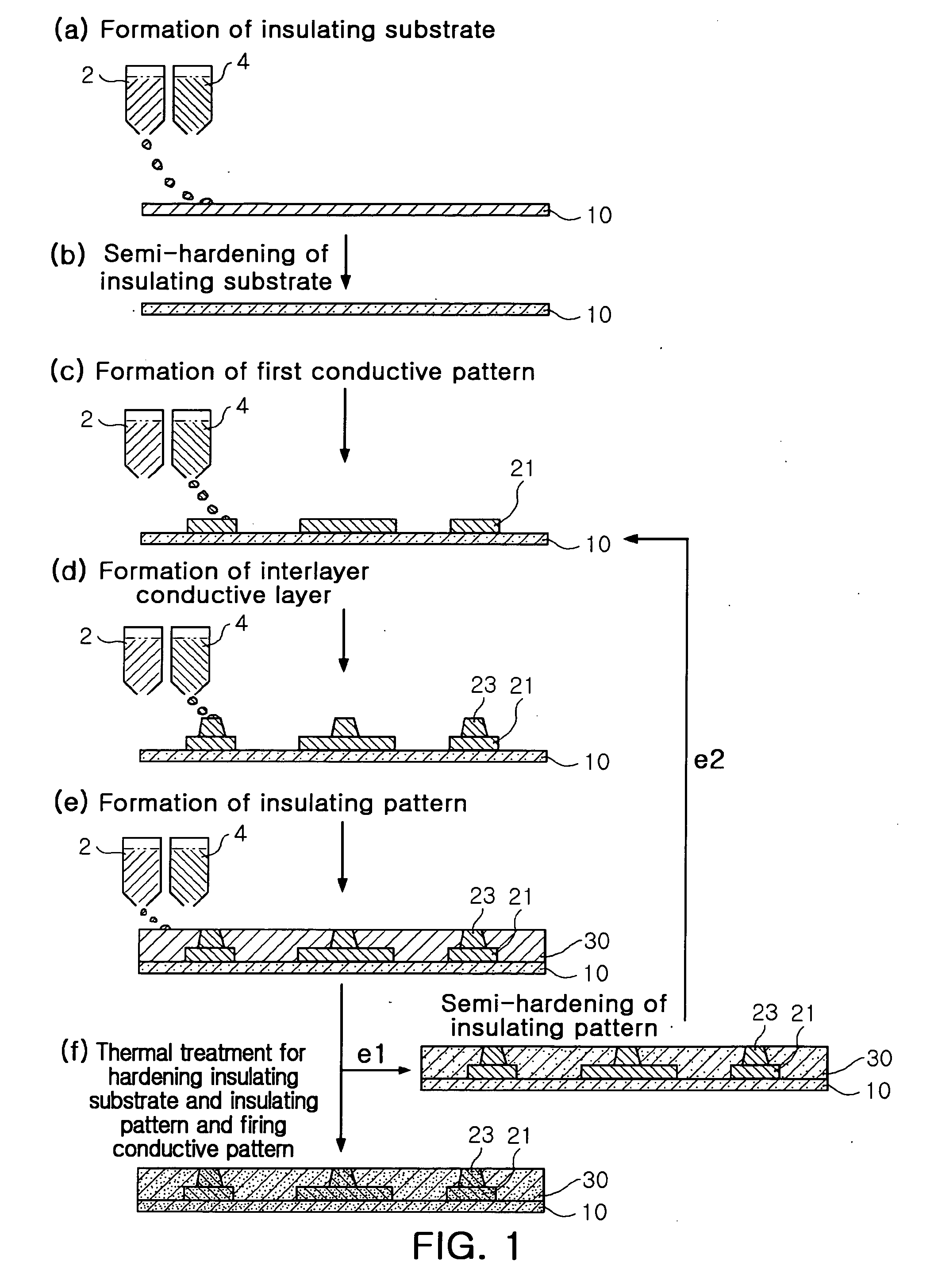
[0077] As shown in FIGS. 1(a) and 1(b), the insulating substrate was formed by printing the insulating ink using the inkjet process and then was dried at 100° C., and was semi-hardened by irradiating UV rays. A...

embodiment 2

[0080] Silver nitride and PVP (MW=10,000) were mixed at a mole ratio of 1:8, and dimethyl formamide (DMF) was added as a reducing agent to a purified water at a volume ratio of 1:1. Then, the reaction was conducted at 100° C. for 30 minutes. Consequently, the conductive ink with 50-nm silver nano particles caped with PVP was prepared.

[0081] 1,1′-(methylene-di-4,1-phenylene)bismaleimide was dissolved in the mixed solution of methyl ethyl ketone (MEK) and dimethyl formamide (DMF) and thus the insulating ink of 15 cps was obtained. PTMA (5-propylsulfonyl-oxyimino-5H-thiophen-2-ylidene)-2-(methylphenyl)-acetonitrile) was used as the photo-polymerization initiator.

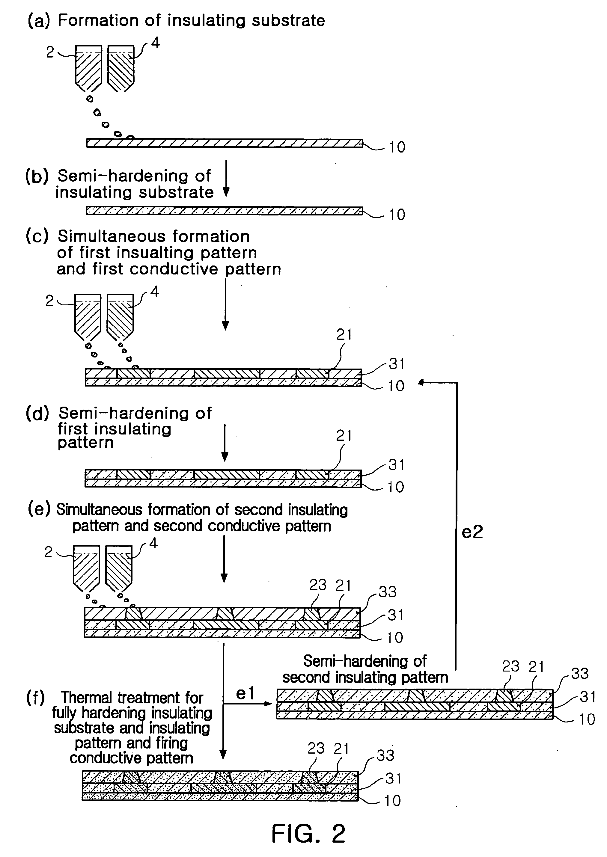
[0082] As shown in FIGS. 2(a) and 2(b), the insulating substrate was formed by printing the insulating ink using the inkjet process and then was dried at 100° C., and was semi-hardened by irradiating UV rays. As shown in FIG. 2(c), the first conductive pattern and the first insulating pattern were formed by printing the condu...


PUM

PropertyMeasurementUnit
Temperatureaaaaaaaaaa
Electrical conductoraaaaaaaaaa
Peel strengthaaaaaaaaaa

Abstract

Provided is a method for manufacturing a printed wiring board, which can enhance the peel strength between an insulating layer and a conductive pattern by a two-step process, that is, a semi-hardening and full-hardening of the insulating layer. In the method for manufacturing the printed wiring board having one or more layers of a conductive pattern and an insulating pattern, an insulating pattern is formed on an insulating substrate, and at least one of the insulating substrate and the insulating pattern is semi-hardened. A conductive pattern is formed on the insulating substrate and/or the insulating pattern, thereby providing a stack structure. Then, a thermal treatment is performed on the stack structure to fully harden the semi-hardened insulating substrate and/or insulating pattern, and the conductive pattern is fired.

Description

RELATED APPLICATION [0001] The present application is based on, and claims priority from, Korean Application Number 2005-118596, filed on Dec. 7, 2005, the disclosure of which is hereby incorporated by reference herein in its entirety. BACKGROUND OF THE INVENTION [0002] 1. Field of the Invention [0003] The present invention relates to a method for manufacturing a printed wiring board, in which a wiring pattern is formed using an inkjet process, and more particularly, to a method for manufacturing a printed wiring board, which can enhance the peel strength between an insulating layer and a conductive pattern by a two-step process, that is, a semi-hardening and full-hardening of the insulating layer. [0004] 2. Description of the Related Art [0005] In the electronic devices, computers, communication devices, and so on, semiconductors or electronic components are mounted on a printed wiring board. Circuit patterns (conductive patterns) of the printed wiring board are highly densified by...

Claims


Application Information

Patent Timeline
IPC IPC(8): H01L21/4763
CPCH05K3/125H05K3/4647H05K3/4664H05K2201/0154H05K2201/09881H05K2203/013B33Y80/00H05K3/10
Inventor CHO, HYE JINJOUNG, JAE WOOOH, SUNG IL
Owner SAMSUNG ELECTRO MECHANICS CO LTD
Why Eureka
Try Eureka