
Method for removing residues formed during the manufacture of MEMS devices

Active Publication Date: 2007-06-14
TELEDYNE DIGITAL IMAGING INC
View PDF8 Cites 54 Cited by
  • Summary
  • Abstract
  • Description
  • Claims
  • Application Information

AI Technical Summary

Benefits of technology

[0036] The present invention allows the removal without stiction of the inorganic fluoride residues (either metal-based or non-metal-based) formed during the Vapor HF release process. It has been found surprisingly that the problems described in the prior art can be overcome by employing an all-dry water vapor cleaning approach to remove the residues and further that satisfactory cleaning can take place at a temperature and pressure well below the critical point for water.

Problems solved by technology

The manufacture of Micro-Electro-Mechanical Systems (MEMS) such as micro-gyroscopes, micro-accelerometers, RF micro-resonators, micro-mirrors, micro-motors, micro-actuators and other such micro-devices integrating very sensitive moving mechanical parts causes a very serious challenge for a number of reasons including the facts that: a. These very sensitive mechanical parts are typically made of silicon (polysilicon or silicon-germanium); b. The sacrificial material underlying these mechanical parts to be released is typically silicon oxide; c. The etch stop layer underlying this silicon oxide sacrificial layer is typically silicon nitride or silicon (polysilicon or silicon-germanium); d. The mechanical release of the mechanical parts requires the removal of the sacrificial material in liquid or vapor HF-based chemistries; e. A liquid HF-based solution does not allow one to perform a release in presence of a CMOS compatible Al metallization scheme; f. A vapor HF-based approach on the other hand leads to undesirable post-release residues that are detrimental to the functionality of the MEMS devices as they block or limit the movements of the released parts.
The selected method must not lead to any stiction that could obviously also be detrimental to the functionality of the devices.
The problem with liquid non-buffered-HF solutions is that they quickly attack the Al-based metallization schemes which are CMOS compatible.
TiN therefore may not be suitable for MEMS applications needing a low interconnection resistance.
The problem with BHF solutions is that improperly rinsed BHF released wafers will result in an undesirable precipitation of solid ammonium fluorosilicate, (NH4)2SiF6 crystals under the released mechanical parts.
Based on the CMOS compatibility requirements, gold (Au), although resistant to liquid HF-based solutions according to Willams et al., could not be considered as it is not CMOS compatible.
Even though a liquid HF-based solution leads to severe issues in presence of metals for CMOS control / actuation electronics, one could circumvent this problem by performing a release prior to the metallization step.
This however also involves many potential issues such as: a. potential metal residues in-between released structures; b. Sputtering of metal is impossible due to item a above; c. Al or other metal evaporation means a lift-off approach in conjunction with the metal evaporation techniques.
Therefore, the resist strip involves liquid exposure during the remaining steps which would leave the devices prone to stiction; and d. Low yield and cross-contamination due to potential breakage of devices along the fabrication processes that could contaminate other products.
Such excessive etch requirements therefore require excessive etch times therefore leading to an attack of the metal schemes to some extent.
Even though performing a Vapor HF release in the conditions used by Ouellet et al. prevents the etch of the metal structures, it still potentially leads to the formation of undesirable fluorine-based by-products that are detrimental to the functionality of the devices as they can potentially block or limit the movements of the MEMS-released structures.
However, none of them (beside Tong et al.) covered the formation of residues due to the exposure of metallized devices to Vapor HF.
However, there is no mention about the potential formation of residues due to such an exposure to a Vapor HF process.
However, it is most likely that in that case the AlF3 residues are swept away (since AlF3 is not soluble in acids) during the Vapor HF process.
However, there is no discussion related to the formation of residues as such residue formation is most likely minimal.
Even though this invention could allow one to remove the inorganic residues formed during the Vapor HF process in presence of Al (or any other metal), this approach presents many drawbacks for MEMS applications, namely: a. As this method is intended for CMOS processes, the wafers are not appropriately dried which would in turn lead to released structures of advanced MEMS devices displaying severe stiction problems; b. Although the “agitation” found in a cascade-type of rinse could allow one to clear the inorganic residues formed during the Vapor HF process, this approach may not be suitable for fragile advanced MEMS devices as it could be prone to breakage due to the harsh mechanical action during a cascade rinse; c. Such an apparatus proposed by Chhabra et al. does not exhibit any flexibility in terms of water temperature nor the possibility to use a gentle “molecular” excitation of the DI water.
However, Ouellet et al. did not address the possibility that their invention could leave some fluorine-based residues behind.

Method used


Image

  • Method for removing residues formed during the manufacture of MEMS devices
  • Method for removing residues formed during the manufacture of MEMS devices
  • Method for removing residues formed during the manufacture of MEMS devices

Examples


Embodiment Construction

Metal-based Residues

[0070] The following comparative examples and examples of the invention demonstrate the advantages of the invention. This exercise was completed by taking into account the most commonly used CMOS-compatible metals in the semiconductor industry such as [0071] Al, Ti, Cu, Ta, W, Co and Ni. [0072] Al-based residues [0073] Al-based residue formation

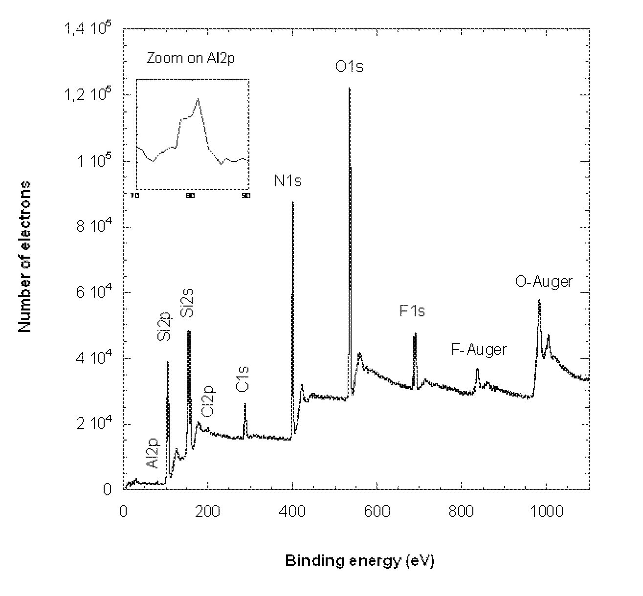
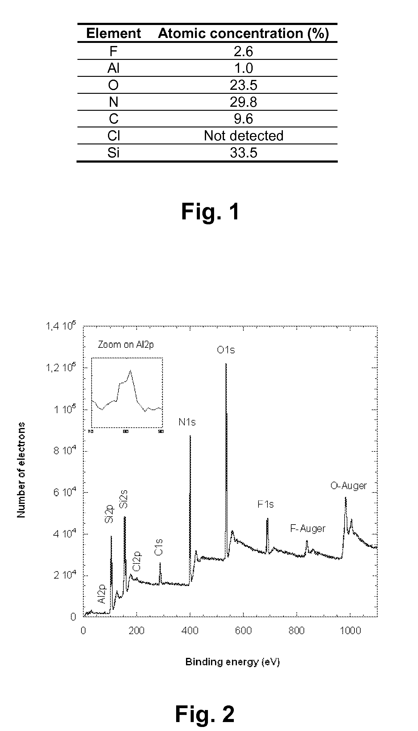
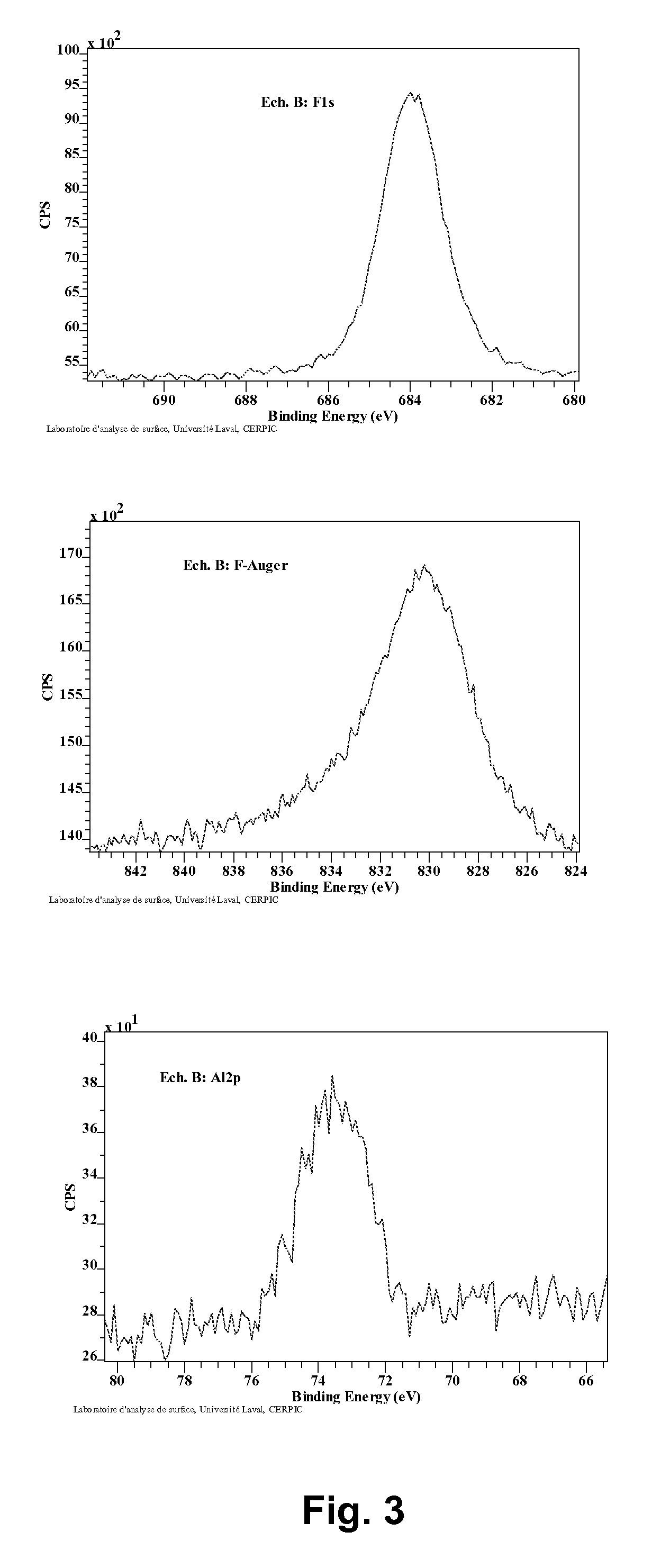
[0074] In the case of a Vapor HF process performed in presence of Al, the XPS analyses data gathered in the field area in-between MEMS devices and shown in FIG. 1 (summary table) and FIG. 2 and FIG. 3 (binding energy spectra) demonstrate that the residues formed is an Al fluoride compound (AlF3) based on 2 observations from the XPS analyses: [0075] a. The F / Al atomic ratio is approximately 3; [0076] b. The Al2p binding energy is of 75.8 eV which is typical for AlF3 compounds.

AlF3 Formation Mechanism

[0077] Although AlF3 has a low solubility of 0.00559 g / cm3 in cold water (25° C.), it is perfectly soluble in hot water ...


PUM


Abstract

A method of removing residues from an integrated device, in particular residues resulting from processing in HF vapor, is disclosed wherein the fabricated device is exposed to dry water vapor for a period of time sufficient to dissolve the residues in the dry water vapor.

Description

CROSS REFERENCE TO RELATED APPLICATION [0001] This application claims the benefit under 35 USC 119(e) of prior U.S. provisional application No. 60 / 699,852, filed Jul. 18, 2005, the contents of which are herein incorporated by reference.FIELD OF THE INVENTION [0002] This invention relates to the field of integrated device manufacture, and in particular to the manufacture of MEMS and like devices. BACKGROUND OF THE INVENTION [0003] The manufacture of Micro-Electro-Mechanical Systems (MEMS) such as micro-gyroscopes, micro-accelerometers, RF micro-resonators, micro-mirrors, micro-motors, micro-actuators and other such micro-devices integrating very sensitive moving mechanical parts causes a very serious challenge for a number of reasons including the facts that: [0004] a. These very sensitive mechanical parts are typically made of silicon (polysilicon or silicon-germanium); [0005] b. The sacrificial material underlying these mechanical parts to be released is typically silicon oxide; [0...

Claims


Application Information

Patent Timeline
IPC IPC(8): H01L21/461H01L21/302
CPCB08B3/08B08B7/00B81C1/00849B81C1/00928H01L21/02068
Inventor FORTIN, VINCENTOUELLET, JEAN
Owner TELEDYNE DIGITAL IMAGING INC
Learn More