Multilayer print circuit board

a print circuit board and multi-layer technology, applied in the direction of electrical apparatus construction details, instruments, program control, etc., can solve the problems of unwanted radiation of electro magnetic waves, adversely affecting the print circuit board, and the noise of the inductance cannot often be decoupled, so as to prevent potential fluctuations.

Inactive Publication Date: 2007-06-14
CANON KK
View PDF10 Cites 47 Cited by
  • Summary
  • Abstract
  • Description
  • Claims
  • Application Information

AI Technical Summary

Benefits of technology

[0018] The present invention has been made in view of the problem described above, and has as its object to effectively prevent potential fluctuation in the power supply terminal of the semiconductor device, that is, noise outflow to the main power supply wiring.

Problems solved by technology

As the speed and frequency of a semiconductor integrated circuit (IC / LSI) increase, EMI (Electro Magnetic Interference) as the unwanted radiation of the electro magnetic wave has become an issue.
Various factors can cause EMI.
Noise outflow to the main power supply wiring adversely affects a print circuit board over a wide range to induce degradation of EMI.
Recently, however, the conventional method of inserting the inductance cannot often decouple the noise, and the noise often flows out to the main power supply.
Even insertion of an inductor 1 to the main power supply side according to the prior art described above cannot solve this phenomenon.

Method used


Image

  • Multilayer print circuit board
  • Multilayer print circuit board
  • Multilayer print circuit board

Examples


first embodiment

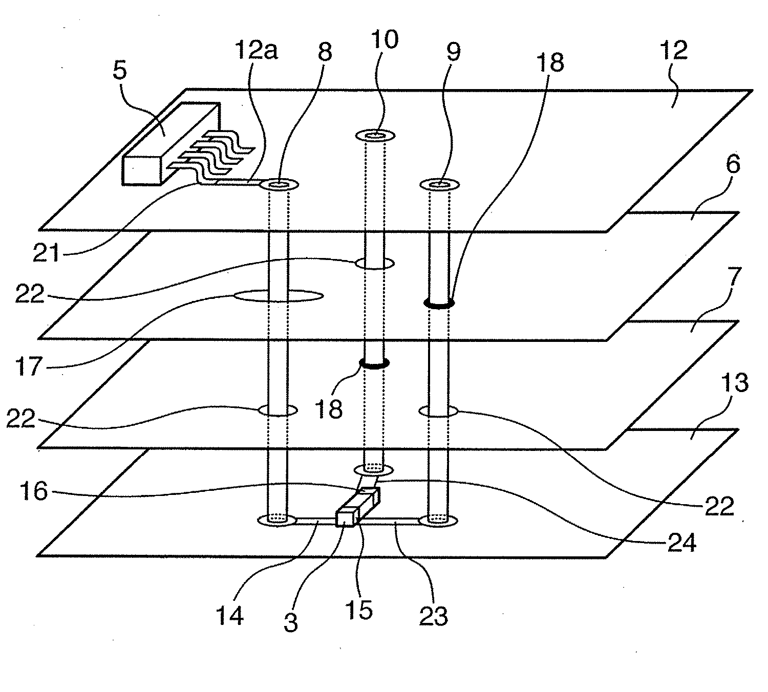
[0041]FIG. 1 is a perspective view schematically showing a multilayer print circuit board according to the first embodiment.

[0042] Referring to FIG. 1, reference numeral 5 denotes a semiconductor device such as an IC or LSI, which is arranged on a first surface layer 12. A wiring pattern 12a extends from a power supply terminal 21 of the semiconductor device 5 and connects to a first power supply via hole 8. The first power supply via hole 8 extends to a second surface layer 13 and connects to a power supply terminal 15 of a bypass capacitor 3 on a second surface layer 13 through a wiring pattern 14.

[0043] The first power supply via hole 8 extends through a main power supply layer 6 and ground layer 7 formed as inner layers. The main power supply layer 6 and ground layer 7 respectively have clearance holes (portions where no conductors are present) 17 and 22 to prevent short-circuiting.

[0044] The power supply terminal 15 of the bypass capacitor 3 connects to a second power supply...

second embodiment

[0050]FIG. 11 is a perspective view schematically showing a multilayer print circuit board according to the second embodiment.

[0051] The second embodiment is different from the first embodiment in the order of a main power supply layer 6 and ground layer 7 as inner layers. A clearance hole 17 formed at a portion where a first power supply via hole 8 extends through the main power supply layer 6 has a large size, as in the first embodiment. In addition, a clearance hole 19 formed at a portion where a ground via hole 10 extends through the main power supply layer 6 also has a large size.

[0052]FIG. 12 is a schematic view, seen from above, of the respective layers of the multilayer print circuit board according to the second embodiment.

[0053]FIG. 13 shows a case that does not adopt the second embodiment.

[0054] A large clearance hole 17 is formed only at a portion where a first power supply via hole 8 extends through a main power supply layer 6. This decreases capacitive coupling bet...

third embodiment

[0059]FIG. 16 is a perspective view schematically showing a multilayer print circuit board according to the third embodiment.

[0060] According to the third embodiment, a first power supply via hole 8 and ground via hole 10 are close to each other. A clearance hole 20 at a portion where the first power supply via hole 8 and ground via hole 10 extend through a main power supply layer 6 has a large size and forms one continuous clearance hole.

[0061]FIG. 17 is a schematic view seen from above of the respective layers of the multilayer print circuit board according to the third embodiment.

[0062] In this manner, when the clearance hole is made large, it decreases the capacitive coupling between the clearance hole and the main power supply layer 6 to prevent noise outflow to the main power supply layer 6. In addition, the first power supply via hole 8 and ground via hole 10 are arranged close to each other to enhance the capacitive coupling between the first power supply via hole 8 and g...


PUM

PropertyMeasurementUnit
conductiveaaaaaaaaaa
sizeaaaaaaaaaa
noiseaaaaaaaaaa

Abstract

This invention effectively prevents potential fluctuation in the power supply terminal of a semiconductor device, that is, noise from flowing out to a main power supply wiring. A multilayer print circuit board includes a first power supply via hole which connects to the power supply terminal of a semiconductor integrated circuit on a first surface layer and extends from the first surface layer to a second surface layer, a ground via hole which connects to a ground conductive layer, extends from the ground conductive layer to the second surface layer, and connects to the first power supply via hole on the second surface layer through a bypass capacitor, a first clearance hole which is formed in a power supply conductive layer, and a second clearance hole which is formed in the ground conductive layer. The first clearance hole is larger than the second clearance hole.

Description

BACKGROUND OF THE INVENTION [0001] 1. Field of the Invention [0002] The present invention relates to a technique to reduce noise in a print circuit board mounted with a semiconductor integrated circuit (IC / LSI). [0003] 2. Description of the Related Art [0004] As the speed and frequency of a semiconductor integrated circuit (IC / LSI) increase, EMI (Electro Magnetic Interference) as the unwanted radiation of the electro magnetic wave has become an issue. Various factors can cause EMI. Noise generated by the power supply terminal of the IC / LSI is one major factor. [0005] Conventionally, a bypass capacitor is provided to decrease the noise generated by the power supply terminal of the IC / LSI. The bypass capacitor stably supplies power to the IC and simultaneously prevents potential fluctuation at the power supply terminal of the IC, that is, outflow of the noise to the main power supply wiring. This is based on the operation (decoupling) that the noise of the power supply terminal return...

Claims


Application Information

Patent Timeline
Patent Type & Authority Applications(United States)
IPC IPC(8): G06F1/00
CPCG06F1/188G06F1/189H05K1/0231H05K1/116H05K3/429Y10T29/49126H05K2201/10545H05K2201/10689Y10T29/49117Y10T29/49165H05K2201/09718
Inventor OHSAKA, TOHRU
Owner CANON KK
Why Eureka
Try Eureka