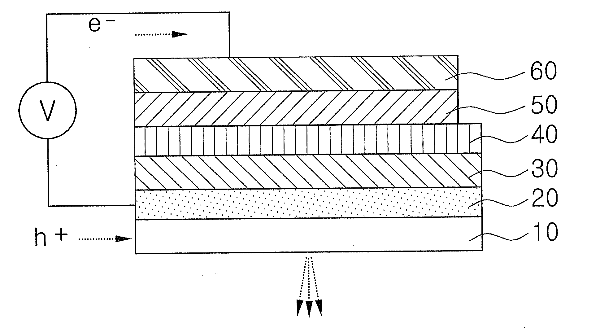
Light emitting device with three-dimensional structure and fabrication method thereof
a technology of light emitting devices and fabrication methods, which is applied in the direction of solid-state devices, electric lighting sources, electric light sources, etc., can solve the problems of reducing the loss of internal light, limiting the increase of internal light, and reducing the amount of light emitted from the device, so as to improve luminescence efficiency and reduce costs.
- Summary
- Abstract
- Description
- Claims
- Application Information
AI Technical Summary
Benefits of technology
Problems solved by technology
Method used
Image

Examples
example 1
[0084]A solution of 1.8424 g of mercaptoacetic acid (MAA) in 8 ml of chloroform was heated to 70° C., and then 3 ml of CdSe semiconductor nanoparticles present at a concentration of 20 mg nanoparticles per ml in toluene (mean nanoparticle diameter 6 nm, available from Evident tech.) were added to the solution with vigorous stirring. Subsequently, the mixture was allowed to react at reflux (70° C.) with stirring for 3 hours. After the reaction was completed, the reaction solution was centrifuged at 3,000 rpm to obtain a precipitate. The precipitate was dispersed in chloroform. The dispersion was again centrifuged at 3,000 rpm for 5 minutes to obtain a precipitate. A cycle of precipitation and dispersion was repeated seven times. The washed semiconductor nanoparticles were dried under vacuum for 6 hours and dispersed in a 0.1 M Tris buffer (pH=9). The dispersion was centrifuged at a g-force of 15,000 g for 10 minutes to remove agglomerates of the semiconductor nanoparticles, and as a ...
experimental example 1
Observation of Surface of Light Emitting Device
[0087]FIG. 5a is a scanning electron micrograph (SEM) of a light emitting device in which a semiconductor nanoparticle layer is formed on the three-dimensional silicon substrate prepared in Example 1. FIG. 5b is an enlarged partial view of FIG. 5a which shows patterned recesses. FIG. 5c is an enlarged partial view of one recess shown in FIG. 5b. The images of FIGS. 5a to 5c reveal that the semiconductor nanoparticles are uniformly adsorbed on the surface of the substrate as well as the inner side walls and bottoms of the recesses. Referring to FIG. 5a, a plurality of the recesses are regularly spaced in the substrate and are formed in a circular lattice pattern.
experimental example 2
Measurement of Amount of Light Emitted from Light Emitting Device
[0088]The amount of light emitted from the light emitting device fabricated in Example 1 was measured by near-field scanning optical microscopy (“NSOM”). The topography of the substrate prepared in Example 1 was obtained by NSOM, and is shown in FIG. 6a. As can be seen from the topography shown in FIG. 6a, a plurality of three-dimensional recesses are regularly spaced and are included in the substrate.
[0089]The light emitting device comprising the semiconductor nanoparticle layer formed on the substrate provided with three-dimensional recesses while maintaining the recessed structure of the substrate was measured for photon intensity by near-field scanning optical microscopy (NSOM). The results are shown in FIG. 6b. Referring to FIG. 6b, as can be seen in the NSOM data, the recesses of the substrate emitted a much larger amount of light than the flat surface of the substrate. The light emitting device prepared accordin...
PUM
 Abstract
Description
Claims
Application Information
 - R&D
- Intellectual Property
- Life Sciences
- Materials
- Tech Scout
- Unparalleled Data Quality
- Higher Quality Content
- 60% Fewer Hallucinations
Browse by: Latest US Patents, China's latest patents, Technical Efficacy Thesaurus, Application Domain, Technology Topic, Popular Technical Reports.
© 2025 PatSnap. All rights reserved.Legal|Privacy policy|Modern Slavery Act Transparency Statement|Sitemap|About US| Contact US: help@patsnap.com