Transistor

a transistor and field-effect technology, applied in the field of field-effect transistors, can solve the problems of sacrificing ease-of-manufacturing for low-voltage operation, and achieve the effects of facilitating the facilitating the fast response of transistors, and facilitating the large flexibility of device architecture and manufacturing process

Inactive Publication Date: 2007-06-21
ACREO
View PDF5 Cites 55 Cited by
  • Summary
  • Abstract
  • Description
  • Claims
  • Application Information

AI Technical Summary

Benefits of technology

[0009] The inventors have unexpectedly found that if the insulating material of traditional OFETs is exchanged for a certain type of polyelectrolytes or oligomeric electrolytes, the properties of the resulting transistor are substantially improved compared to known transistors.
[0043] One way of minimizing the penetration of charge carriers from the electrolyte into the organic semiconductor is to arrange the electrolyte such that it dissociates into smaller and substantially larger ion-complexes. Where the smaller ion-complexes have a first electric charge and the larger ion-complexes have the opposite electric charge, and the voltage applied to the gate electrode is arranged such that it attracts the smaller ion-complexes. These large ion-complexes preferably comprises long polymer chains or large molecules. The size of the larger ion-complexes either prevents them from penetration into the organic semiconductor, and / or makes them substantially immobile, such that they do not migrate to the interface between said electrolyte and said organic semiconductor to any significant extent. This effect is also achieved when the voltage applied to the gate electrode is not sufficiently high to effectuate any substantial displacement of the larger ion-complexes. In other words, the mobility of an ion is a combination of their size and the applied electric field.

Problems solved by technology

These latter approaches sacrifice ease-of-manufacturing for low-voltage operation.

Method used


Image

  • Transistor
  • Transistor
  • Transistor

Examples


second embodiment

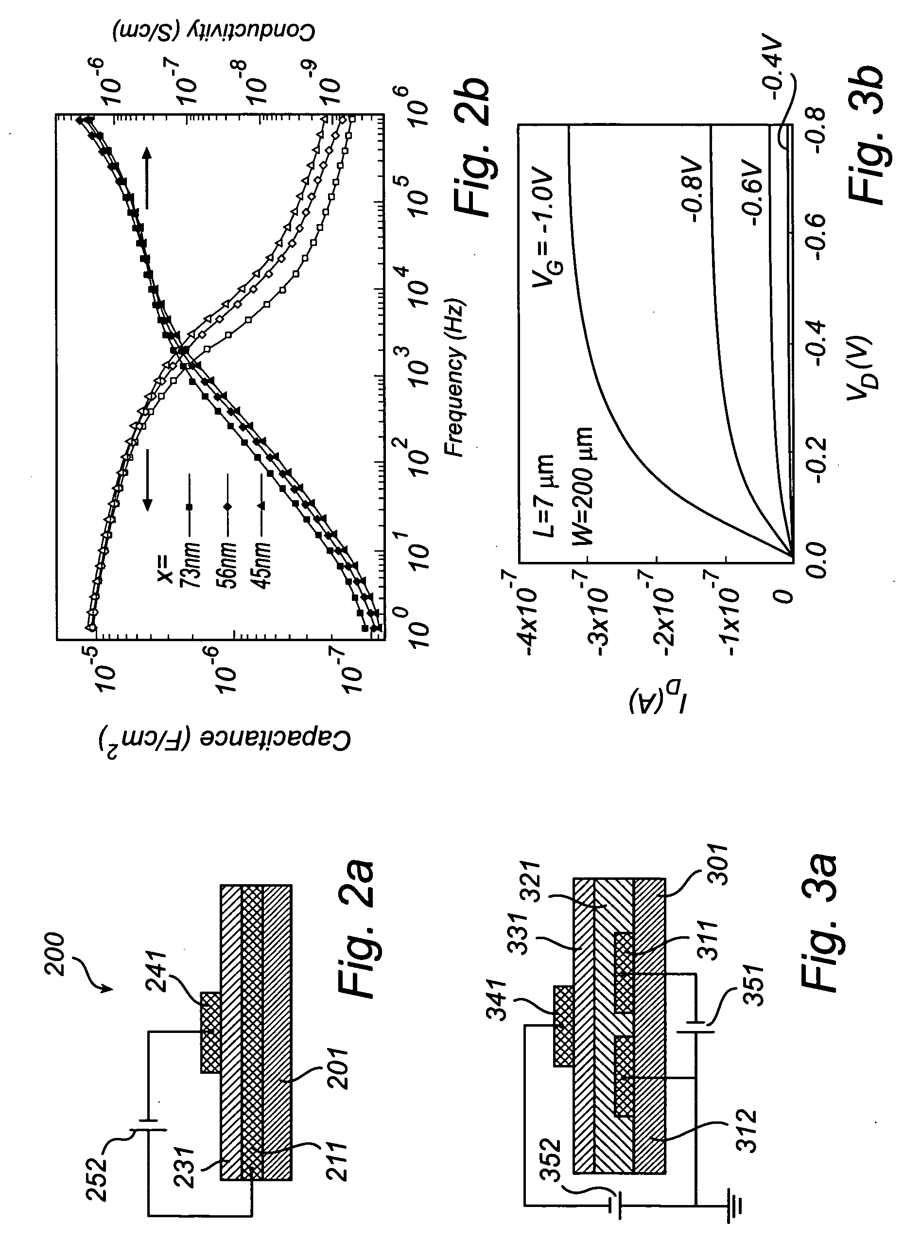
[0067] According to the electrolyte model, a polymer transistor gated via a polyanion electrolyte normally do not depend significantly on the thickness of the “dielectric” layer, nor on the position of the gate electrode. FIG. 4a schematically illustrates the invention, equal to the embodiment described in relation to FIGS. 1 and 3a, except that the gate electrode (441b) is laterally displaced a distance D from the position illustrated in FIGS. 1 and 3a, respectively. The distance between the channel and the gate electrode was varied between 1.25 and 10 mm. In other words, instead of using the designated gate electrode (441a) positioned on top of the channel, the gate electrodes of neighbouring transistor structures was used, i.e. the conventional source and drain electrodes (411;412) together with the neighbouring gate electrode (441b). The (I-V) relationship of the transistor illustrated in FIG. 4a is described in FIG. 4b. Although the channel current level is smaller, due to a po...

third embodiment

[0068] schematically illustrated by FIG. 5a, a much thicker P(VPA-AA) layer (531) is cast from a drop on P3HT (521). More specifically, a drop of concentrated P(VPA-AA) solution is deposited on top of the channel and let for 10 min at 110° C. This results in a hemispherically shaped gate insulator (531). A metal wire, contacted to the polyelectrolyte, is used as a gate electrode. The transistor behavior is similar to those of the transistors illustrated in the previous figures, although high leakage currents were recorded at VG=0 V.

fifth embodiment

[0069] In the invention another class of polyelectrolyte materials, poly(styrene sulfonate) (PSS), has also been tested. PSS was spin coated on top of P3HT giving a thickness of about 100 mm. A Titanium gate electrode was prepared using the same method as for the above described transistors. A schematic cross section of the device is shown in FIG. 6a. Actually, two different PSS-based polymers have been tested: poly(styrene-4-sulfonic acid) (PSSH) and poly(sodium 4-styrenesulfonate) (PSSNa). The latter polymer is the sodium salt of the first polymer. In PSSNa it is probably mainly Na+-ions, instead of protons that migrate through the polyelectrolyte film towards the gate electrode when a negative gate potential is applied. As a consequence, PSSNa-based transistors are slower than PSSH-based. FIG. 7a is a diagram showing ID vs. VD for a P3HT transistor with an about 100 nm thick PSSNa gate insulator, measured in humid air (relative humidity ˜40%) at room temperature. FIG. 7b illustra...


PUM


Abstract

A fast organic field effect transistor (100), which operates at low voltages, is achieved by the introduction of an oligomeric or polymeric electrolyte (131) between the gate electrode (141) and the organic semiconductor layer (121), which electrolyte (131) has a dissociation constant of at least 10−8. Said organic semiconductor layer (121) is in contact with the source electrode (111) and the drain electrode (112) of the transistor. In operation a potential (152) applied to said gate electrode (141) controls the current A between said source electrode (111) and said drain electrode (112).

Description

PRIORITY STATEMENT [0001] This application claims benefit of priority under 35 U.S.C. § 119 from European Patent Application No. 05110565.8 filed on Nov. 9, 2006, in the European Patent Office, the disclosure of which is incorporated herein by reference in its entirety. TECHNICAL FIELD [0002] The invention relates generally to Field-Effect Transistors (FET) and more specifically to Organic Field-Effect Transistors. BACKGROUND ART [0003] There are two main categories of organic transistors: electrochemical transistors (ECT) and field-effect transistors (FET). [0004] Typically, in an ECT the transistor channel is formed of an electrochemically active layer, and the conductivity of the transistor channel is altered by changing its electrochemical redox state (electrochemical doping). In other words, one oxidation state of the channel corresponds to low channel conductivity (the transistor is OFF), while the other oxidation state corresponds to high channel conductivity (the transistor ...

Claims


Application Information

Patent Timeline
Patent Type & Authority Applications(United States)
IPC IPC(8): H01L29/08H01L31/00
CPCH01L51/002H01L51/0516H01L51/0541H10K71/30H10K10/468H10K10/464
Inventor HERLOGSSON, LARSGUSTAFSSON, GORANHAGEL, OLLE-JONNYSANDBERG, MATSBERGGREN, MAGNUSCRISPIN, XAVIERROBINSON, NATHANIEL
Owner ACREO
Why Eureka
Try Eureka