Image sensor and method of driving transfer transistor of image sensor

a technology of image sensor and transfer transistor, which is applied in the direction of radio frequency control devices, instruments, television systems, etc., can solve the problems of increasing dark current, deteriorating image quality, and increasing fixed pattern noise, so as to reduce noise and dark current

Active Publication Date: 2007-06-28
ELECTRONICS & TELECOMM RES INST
View PDF11 Cites 29 Cited by
  • Summary
  • Abstract
  • Description
  • Claims
  • Application Information

AI Technical Summary

Benefits of technology

[0034] Unlike a conventional technique adapted to fully deplete a photodiode, in the present invention, the amount of charge remaining in the channel region of the transfer transistor is not affected by other charges when the transfer transistor is turned on. Accordingly, when the photodiode is transfer state, the amount of charge remaining in the photodiode gets constant, and an influence on the amount of charge in the photodiode and the amount of charge transferred by the transfer transistor is minimized, thus reducing noise and dark current. In the present invention, when turned on, the transfer transistor operates at a predetermined pseudo pinch-off voltage so that the amount of charge remaining in the source of the transfer transistor is unchanged.

Problems solved by technology

Such a nonuniform amount of electrons from the floating diffusion node causes irregularity of the reset condition, thus deteriorating the quality of an image.
Unstable reset and transfer operations of the transfer transistor may cause two typical problems of increased dark current and increased fixed pattern noise.
However, as a modern semiconductor process and device is scaled down and an operating voltage is reduced, the floating diffusion node voltage gets gradually lower.
Accordingly, a pinning voltage of a pinned photodiode gets lower, thereby deteriorating a pixel characteristic such as well capacity.
Further, a voltage barrier necessarily exists between the pinned photodiode and the channel of the transfer transistor to some extent.
When the barrier is not sufficiently reduced, the pinned photodiode is not completely reset, which may cause more severe problems.
In addition, the well capacity may be lowered and resetting (e.g., depletion) may be insufficient.
However, the voltage boosting circuit applies a voltage over a normal operation condition, which may degrade the reliability of a gate oxide.
Further, this approach has a limitation of characteristic enhancement in a complete reset condition.

Method used


Image

  • Image sensor and method of driving transfer transistor of image sensor
  • Image sensor and method of driving transfer transistor of image sensor
  • Image sensor and method of driving transfer transistor of image sensor

Examples


first exemplary embodiment

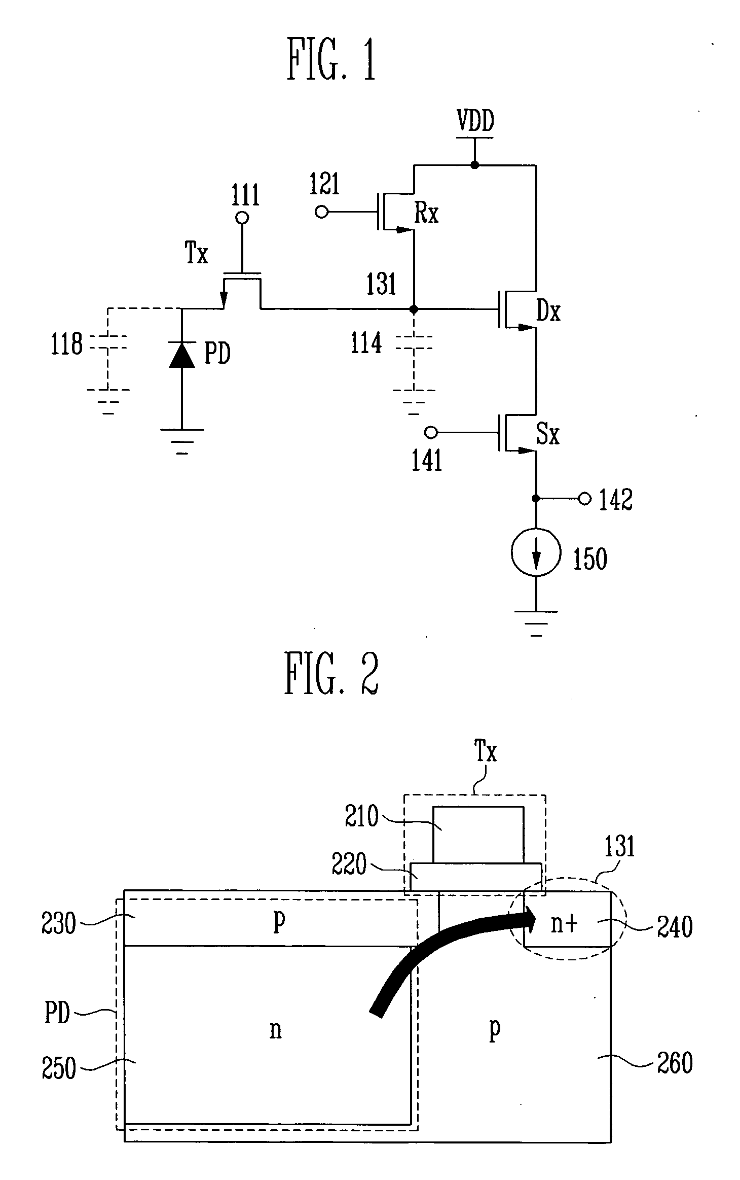
[0048] An image sensor of this embodiment includes: a photodiode; a photosensitive pixel including a transfer transistor for transferring photon-induced charges created in the photodiode to a floating diffusion node; and a voltage control unit for applying a switching signal having a pseudo pinch-off voltage lower than the power supply voltage or a rising time that is two times or greater than the minimum rising time, to the gate of the transfer transistor during a partial or entire section of a turn-on section of the transfer transistor. Preferably, the pseudo pinch-off voltage ranges from a value several hundreds of mV lower than the power supply voltage to a half the power supply voltage.

[0049] In the case where this embodiment is implemented by a CMOS image sensor, it may be applied to the 4-transistor pixel structure shown in FIG. 1. Once a pseudo pinch-off voltage value to be generated by a voltage control unit is determined, the control unit may be implemented using a variet...

second exemplary embodiment

[0072] An image sensor of this embodiment includes a transfer transistor for transferring photon-induced charges created in the photodiode to a floating diffusion node, and a reset transistor for resetting the floating diffusion node, in which, a voltage applied to a drain and / or gate of the reset transistor is changed to control the channel voltage of the transfer transistor to be lower than the floating diffusion node voltage so that the transfer transistor operates in a pseudo pinch-off mode.

[0073] Here, the turn-on voltage of the transfer transistor may be a power supply voltage. Preferably, the voltage applied to the drain and / or gate of the reset transistor may range from a value several hundreds of mV higher than the power supply voltage to a value 1.5 times higher than the power supply voltage.

[0074] When this embodiment is implemented by a CMOS image sensor, it may be applied to the 4-transistor pixel structure shown in FIG. 1. It can be seen that even in the image sensor...

third exemplary embodiment

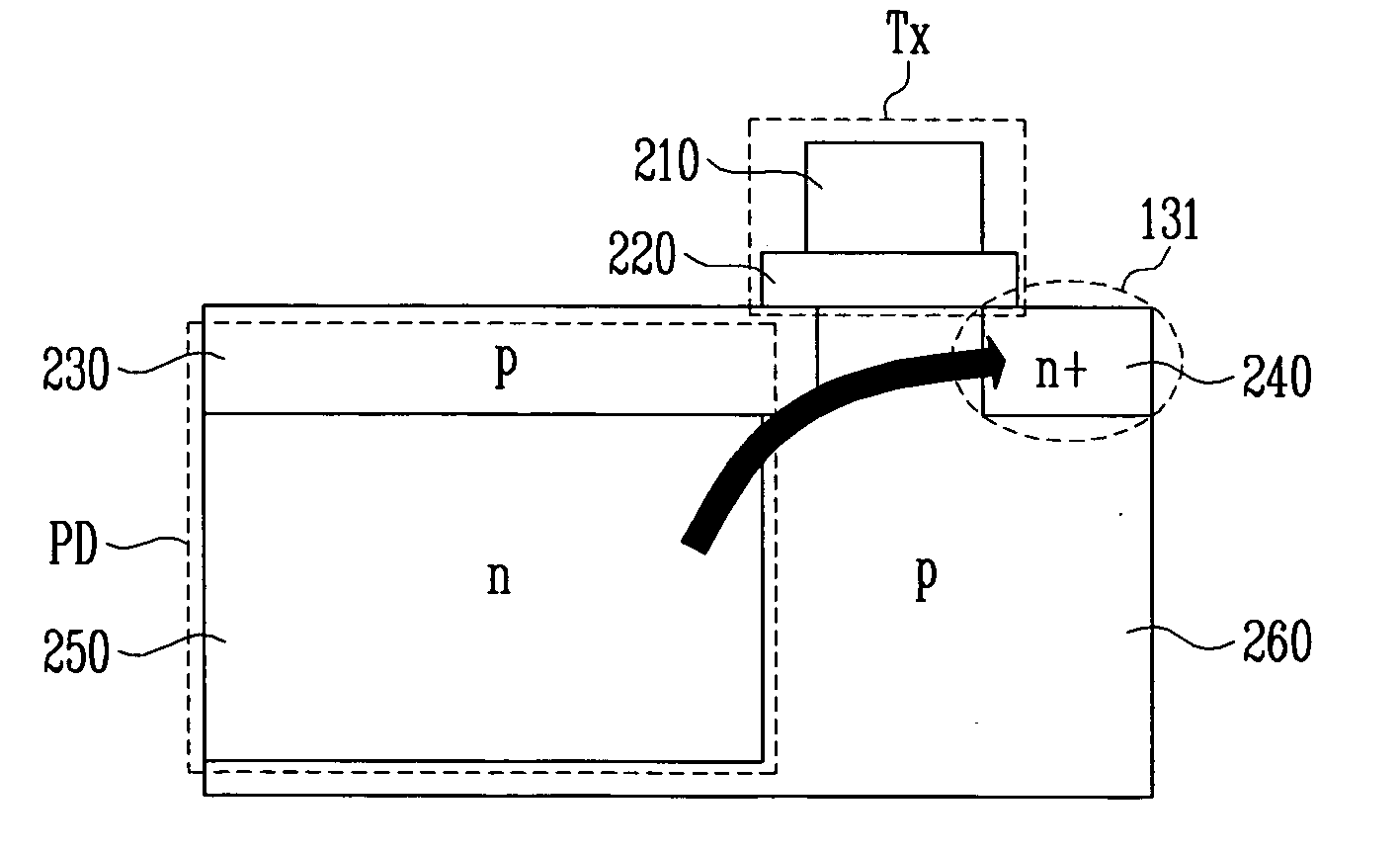
[0080]FIG. 3 shows a structure of a photodiode and a transfer transistor of a CMOS image sensor having an enhanced structure to which a method of driving a transfer transistor according to this exemplary embodiment may be applied. In this embodiment, a switching signal applied to the gate of the transfer transistor includes a turn-on voltage that is enhanced as in the first embodiment, and a turn-off voltage that is a lower negative offset voltage than a ground voltage in order to optimize the performance of the image sensor.

[0081] A method of applying a pseudo pinch-off voltage and the resulting effect are the same as in the first embodiment, and thus the enhanced structure of the transfer transistor, a method of applying a negative offset voltage, and the resulting effect will be described herein.

[0082] Only the photodiode PD, the transfer transistor Tx, and the floating diffusion region 131 of the 4-transistor pixel are shown in FIG. 3. The transfer transistor Tx includes a gat...


PUM


Abstract

Provided is a 4-transistor CMOS image in which a driving condition or a pixel structure is changed so that a transfer transistor in a pixel operates in a pinch-off condition during reset and transfer operations in order to reduce dark current and fixed-pattern noise caused by a change in an operation condition of the transfer transistor and inter-pixel characteristic discrepancy. The image sensor includes a photosensitive pixel including a transfer transistor for transferring photon-induced charges created in a photodiode; and a voltage control unit for controlling a turn-on voltage applied to a gate of the transfer transistor to be lower than a floating diffusion node voltage plus the threshold voltage of the transfer transistor during a partial or entire section of a turn-on section of the transfer transistor such that the transfer transistor operates in a pseudo pinch-off mode.

Description

CROSS-REFERENCE TO RELATED APPLICATION [0001] This application claims priority to and the benefit of Korean Patent Application No. 2005-119493, filed Dec. 8, 2005, and 2006-98889, filed Oct. 11, 2006, the disclosure of which is incorporated herein by reference in its entirety. BACKGROUND [0002] 1. Field of the Invention [0003] The present invention relates to an image sensor and a method of driving a transfer transistor of the image sensor that transfers photon-induced charges, and more particularly, to an image sensor and a method of driving a transfer transistor of the image sensor that are capable of maintaining a depletion degree of charges in a photodiode when the photodiode is reset. [0004] 2. Discussion of Related Art [0005] Image sensors may be classified into a charged coupled device (CCD) sensor and a complementary metal oxide semiconductor (CMOS) image sensor, which use electron-hole pairs separated by light having an energy higher than a silicon band gap, in which an amo...

Claims


Application Information

Patent Timeline
Patent Type & Authority Applications(United States)
IPC IPC(8): H01L27/00H04N5/361H04N5/3745
CPCH01L27/14603H01L27/14609H04N5/361H04N5/3745H04N25/626H04N25/60H04N25/63H04N25/77H01L27/146
Inventor MHEEN, BONGKIM, MISONG, YOUNG
Owner ELECTRONICS & TELECOMM RES INST
Why Eureka
Try Eureka