
MIM capacitor structure and method of manufacturing the same

a technology of metal insulation metal and capacitors, which is applied in the direction of capacitors, semiconductor devices, electrical equipment, etc., can solve the problems of loss of electric charges and decrease of capacitance of capacitors, and achieve the effect of small leakage curren

Inactive Publication Date: 2007-06-28
IND TECH RES INST
View PDF5 Cites 13 Cited by
  • Summary
  • Abstract
  • Description
  • Claims
  • Application Information

AI Technical Summary

Benefits of technology

[0006]Accordingly, at least one objective of the present invention is to provide a metal-insulator-metal (MIM) capacitor structure having a smaller leakage current.
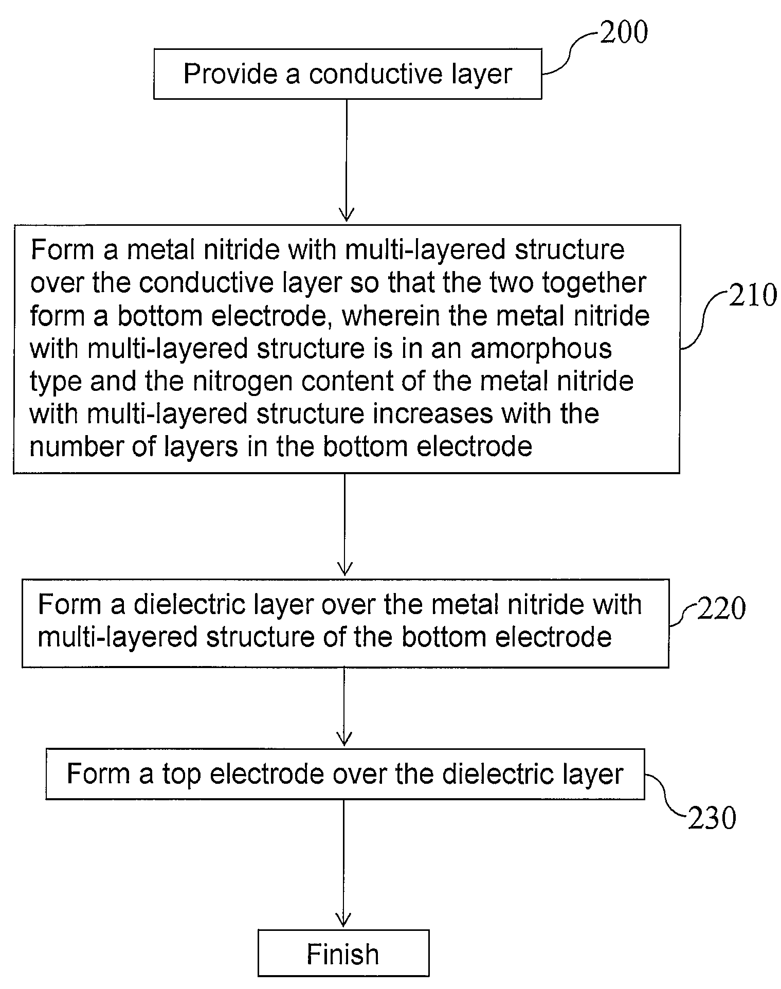
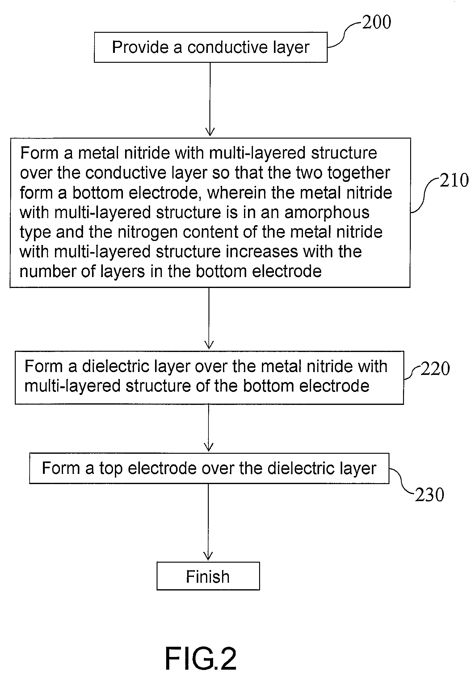
[0007]At least another objective of the present invention is to provide a method for fabricating a metal-insulator-metal (MIM) capacitor that can improve the quality of the capacitor and significantly increase the applicability of using high dielectric constant film material in DRAM capacitor devices.
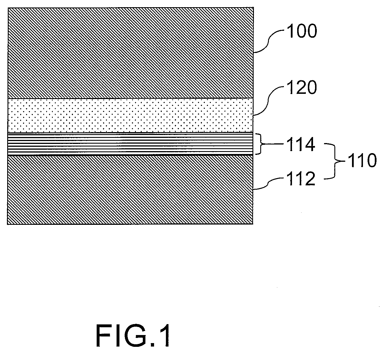
[0010]In the present invention, the bottom electrode close to the dielectric layer is fabricated using an amorphous metal nitride with multi-layered structure and the nitrogen content within the metal nitride with multi-layered structure gradually increases toward the direction of the dielectric layer. Hence, the degree of crystallinity in the dielectric layer is substantially reduced and further the quality of the capacitor is significantly improved.

Problems solved by technology

However, during the process of fabricating the capacitor, a crystalline electrode material often induces its overlying insulating material to crystallize.
The reason for this is that the presence of grain boundaries inside the crystalline material is a significant factor for the loss of electric charges.
Furthermore, the thermal stability of the capacitor in a subsequent high-temperature treatment of the transistor fabrication will deteriorate, and ultimately, the capacitance of the capacitor will decrease.

Method used


Image

  • MIM capacitor structure and method of manufacturing the same
  • MIM capacitor structure and method of manufacturing the same
  • MIM capacitor structure and method of manufacturing the same

Examples


Embodiment Construction

[0015]Reference will now be made in detail to the present preferred embodiments of the invention, examples of which are illustrated in the accompanying drawings. Wherever possible, the same reference numbers are used in the drawings and the description to refer to the same or like parts.

[0016]FIG. 1 is a schematic cross-sectional view of a metal-insulator-metal (MIM) capacitor structure according to one embodiment of the present invention. As shown in FIG. 1, the metal-insulator-metal (MIM) capacitor includes a top electrode 100, a bottom electrode 110 and a dielectric layer 120. The dielectric layer 120 is disposed between the top electrode 100 and the bottom electrode 110. Furthermore, the bottom electrode 110 comprises a conductive layer 112 and a metal nitride with multi-layered structure 114. The metal nitride with multi-layered structure 114 is disposed between the conductive layer 112 and the dielectric layer 120. The nitrogen content within the metal nitride with multi-layer...


PUM

PropertyMeasurementUnit
conductiveaaaaaaaaaa
thicknessaaaaaaaaaa
dielectric constantaaaaaaaaaa

Abstract

A metal-insulator-insulator (MIM) capacitor structure is provided. The MIM capacitor includes a top electrode, a bottom electrode and a dielectric layer. The dielectric layer is disposed between the top electrode and the bottom electrode. The main feature for this kind of MIM capacitor is that the bottom electrode includes a conductive layer and a metal nitride with multi-layered structure. The metal nitride with multi-layered structure is disposed between the conductive layer and the dielectric layer. The nitrogen content in the metal nitride with multi-layered structure gradually increases toward the dielectric layer and the metal nitride belongs to the amorphous type. Due to the presence of the metal nitride, the dielectric layer is prevented from crystallization, thereby reducing the current leakage of the MIM capacitor.

Description

CROSS-REFERENCE TO RELATED APPLICATION[0001]This application claims the priority benefit of Taiwan application serial no. 94146470, filed Dec. 26, 2005. All disclosure of the Taiwan application is incorporated herein by reference.BACKGROUND OF THE INVENTION[0002]1. Field of the Invention[0003]The present invention relates to a metal-insulator-metal (MIM) capacitor and method of manufacturing the same. More particularly, the present invention relates to a metal-insulator-metal (MIM) capacitor structure and method of manufacturing the same that can avoid bottom electrode induced crystallization of the insulator.[0004]2. Description of the Related Art[0005]Metal-insulator-metal (MIM) capacitor has gradually become the capacitor for the next generation of dynamic random access memory (DRAM). Furthermore, using high dielectric constant (high-k) material to fabricate the insulation layer, sufficient capacitance can be obtained when the capacitor area is reduced. Because electrode material...

Claims


Application Information

Patent Timeline
Patent Type & Authority Applications(United States)
IPC IPC(8): H01L29/00
CPCH01L28/65H01L28/75
Inventor WANG, CHING-CHIUNLIN, CHA-HSINLO, WEN-MIAOLEE, LURNG-SHEHNG
Owner IND TECH RES INST
Learn More