

Memory with resistance memory cell and evaluation circuit
a memory cell and resistance technology, applied in the field of memory circuits, can solve the problems of high current demand, difficult miniaturization of semiconductor memory concepts based on storage capacitors, etc., and achieve the effect of simple and reliable evaluation operation
- Summary
- Abstract
- Description
- Claims
- Application Information
AI Technical Summary
Benefits of technology
Problems solved by technology
Method used
Image

Examples
Embodiment Construction
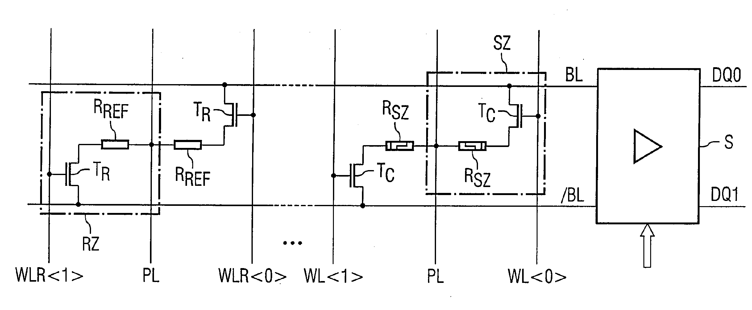
[0025]FIG. 1 schematically shows a detail from a data memory comprising a memory circuit according to the invention. In this case, the memory is preferably formed in matrix-type fashion with column-type word lines and row-type bit lines, the individual memory cells being arranged at the crossover points between word and bit lines. FIG. 1 in this case shows a bit line pair, comprising a bit line BL and a complementary bit line / BL, which are crossed by word lines WL. A multiplicity of memory cells SZ (only two are shown) and two reference memory cells RZ are alternately connected at the crossover points between the bit line BL and the complementary bit line / BL of the bit line pair with the word lines.
[0026] The bit line BL and the complementary bit line / BL are furthermore connected to a differential sense amplifier SA, which compares the electrical potentials on the bit line BL and the complementary bit line / BL with one another and, depending on the resulting potential difference...
PUM
 Abstract
Description
Claims
Application Information