Method for Manufacturing Direct Bonded SOI Wafer and Direct Bonded SOI Wafer Manufactured by the Method

a technology of direct bonded soi and manufacturing method, which is applied in the direction of semiconductor/solid-state device manufacturing, basic electric elements, electric apparatus, etc., can solve the problems of increasing the number of processes and lowering the product yield, and achieve the effect of reducing the product yield

Active Publication Date: 2007-06-28
SUMCO CORP
View PDF8 Cites 34 Cited by
  • Summary
  • Abstract
  • Description
  • Claims
  • Application Information

AI Technical Summary

Benefits of technology

[0012] With the method for manufacturing a direct bonded SOI wafer described in claim 1, since the entire buried oxide film layer is covered by a main surface on the laminating side of the support wafer and the single crystal silicon layer, the side of the buried oxide film is not exposed. Also, since a process for the gas phase expitaxy is not added, the manufacturing cost can be reduced.
[0014] With the method for manufacturing a direct bonded SOI wafer described in claim 2, by removing the oxide film formed on the circumferential end edge and the chamfered portion, drop of product yield caused by the oxide film exposed from the side face can be prevented, and since the oxide film is left only on the laminating surface except the circumferential end edge, a high-quality SOI wafer can be obtained.

Problems solved by technology

Silicon pieces generated by this might become particles, adhere to the surface of the single crystal silicon layer 1 in the active area and cause a pattern defect or other defects in laminated films, which results in a problem that the product yield is lowered.
Also, in the case of epitaxial growth, poly-silicon grows in an exposed oxide film portion, which results in a problem that particles are generated in the fluorinated acid processing process.
However, with the method disclosed in the Patent Document 1, there is a problem that the manufacturing cost is raised by increase in the number of processes since a process for covering the end edges from which the buried oxide films are exposed after bonding by a gas phase epitaxy and a process for removing a film formed by the gas phase epitaxy are added to processes generally performed in the bonding method.

Method used


Image

  • Method for Manufacturing Direct Bonded SOI Wafer and Direct Bonded SOI Wafer Manufactured by the Method
  • Method for Manufacturing Direct Bonded SOI Wafer and Direct Bonded SOI Wafer Manufactured by the Method
  • Method for Manufacturing Direct Bonded SOI Wafer and Direct Bonded SOI Wafer Manufactured by the Method

Examples


Embodiment Construction

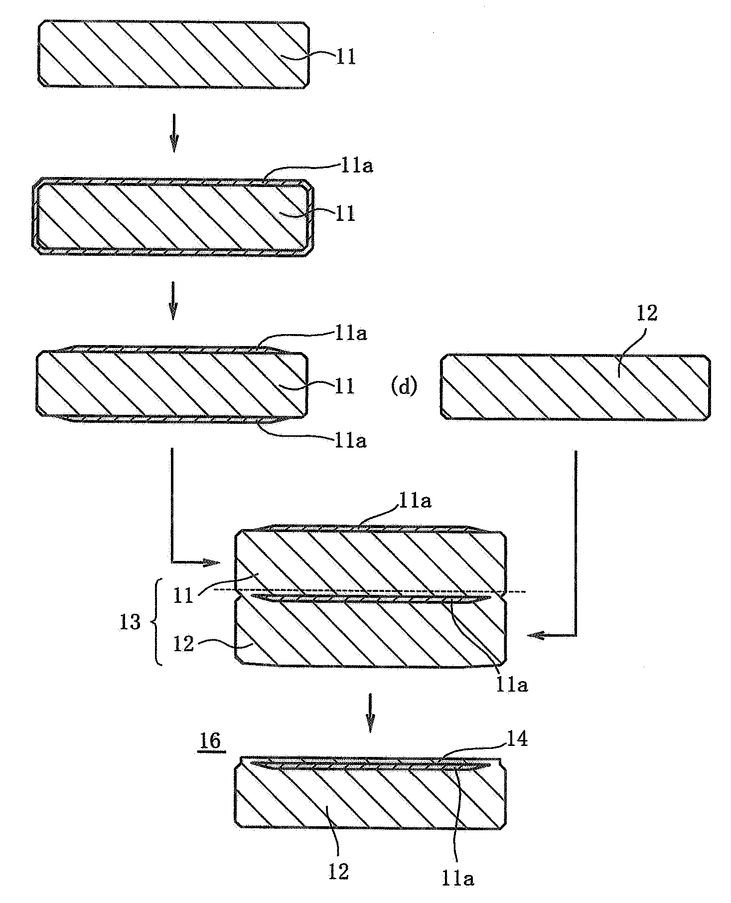
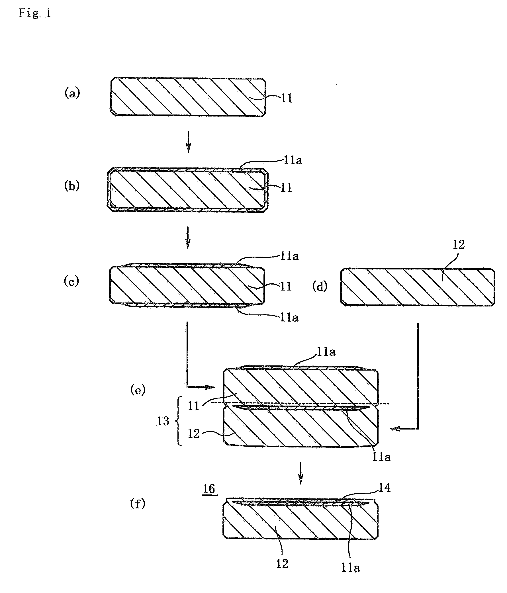
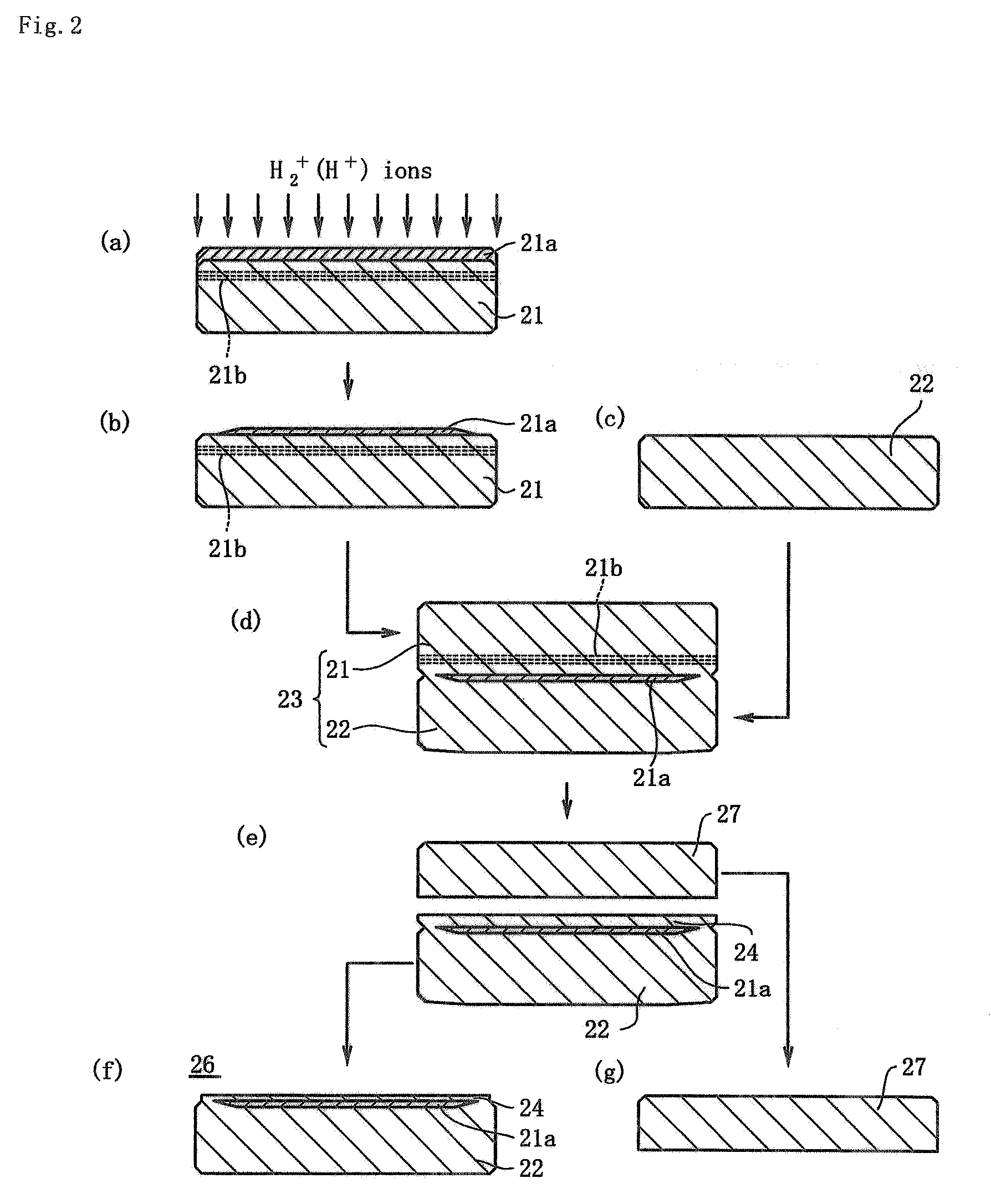
[0040] Next, the method for manufacturing a direct bonded SOI wafer according to the present invention will be described below.

[0041] A method for manufacturing a direct bonded SOI wafer of the present invention is improvement of a method for manufacturing a direct bonded SOI wafer comprising the process of (A) forming a laminated body by laminating a semiconductor wafer and a support wafer via an oxide film; and (B) forming a thin-film single crystal silicon layer on the support wafer using a buried oxide film layer by film-thinning the semiconductor wafer to a predetermined thickness, wherein in a process (C) the entire buried oxide film layer is covered by a main surface on the laminating side of the support wafer and the single crystal silicon layer. Since the entire buried oxide film layer is covered by the main surface of the support wafer on the laminating side and the single crystal silicon layer, the side face of the buried oxide film is not exposed. Also, since a process ...


PUM


Abstract

There are provided a method for manufacturing a direct bonded SOI wafer in which the entire buried oxide film layer is covered and not exposed and a direct bonded SOI wafer. This is the improvement of a method for manufacturing a direct bonded SOI wafer comprising the process of (A) forming a laminated body by laminating a semiconductor wafer and a support wafer via an oxide film; and (B) forming a thin-film single crystal silicon layer on the support wafer using a buried oxide film layer by film-thinning the semiconductor wafer to a predetermined thickness, wherein in a process (C) the entire buried oxide film layer is covered by a main surface on the laminating side of the support wafer and the single crystal silicon layer. The covering of the entire buried oxide film layer is carried out by, between process (A) and (B), removing the oxide film formed on the circumferential end edge of the main surface on the laminating side and the chamfered portion to leave the oxide film only on the laminated surface except the circumferential end edge.

Description

BACKGROUND OF THE INVENTION [0001] 1. Field of the Invention [0002] The present invention relates to a method for manufacturing a direct bonded SOI (Silicon On Insulator) wafer by bonding two silicon wafers via a silicon oxide film, a so-called direct bonded SOI wafer manufacturing method and a direct bonded SOI wafer manufactured by the method. The present invention relates more particularly to a method for manufacturing a direct bonded SOI wafer in which the entire buried oxide film layer is covered and is not exposed and a direct bonded SOI wafer manufactured by the method. [0003] 2. Description of the Related Art [0004] With high integration, high performance, multi-functions and high reliability of a semiconductor integrated circuit, a dimension of a pattern has become increasingly finer. With this, an SOI wafer having a thin-filmed SOI layer without a defect on a wafer surface layer to be a device-forming area with an oxide film layer between them is in demand. As a method for...

Claims


Application Information

Patent Timeline
Patent Type & Authority Applications(United States)
IPC IPC(8): H01L21/30
CPCH01L21/2007H01L21/76251H01L21/76254
Inventor MORITA, ETSUROUOKAWA, SHINJIONO, ISOROKU
Owner SUMCO CORP
Why Eureka
Try Eureka