Method of fabricating nanodevices

a nano-device and nano-structure technology, applied in the field of nano-fabrication, can solve the problems of affecting the production efficiency of nano-devices, affecting the quality of nano-devices, so as to achieve the effect of large-scale mass production and large-scale mass production

Active Publication Date: 2007-06-28
FEI CO
View PDF21 Cites 9 Cited by
  • Summary
  • Abstract
  • Description
  • Claims
  • Application Information

AI Technical Summary

Benefits of technology

[0014] What is needed is an improved method of manufacturing certain nanodevices, including CNT electron sources, so that they can be mounted into a macroscopic device in a repeatable, reliable manner suitable for large-scale mass production.
[0015] It

Problems solved by technology

Assembly of nanoparticles or nanostructures into nanodevices presents significant problems, however, because the individual components or subunits are very small.
Manipulation of individual nanoparticles, even when possible, is slow and tedious.
Unfortunately, these techniques are better suited for use in laboratories than for large-scale mass-production of nanodevices.
These sources have a relatively large energy spread of the emitted electrons, which negatively impacts the resolution of the microscope.
It is very difficult to obtain a stable electron current from such tips except in extremely good vacuum because of contamination, shape changes due to surface migration of the metal atoms, and the unavoidable bombardment by ions that are created when an electron beam is drawn from the source.
Unfortu

Method used


Image

  • Method of fabricating nanodevices
  • Method of fabricating nanodevices
  • Method of fabricating nanodevices

Examples


Embodiment Construction

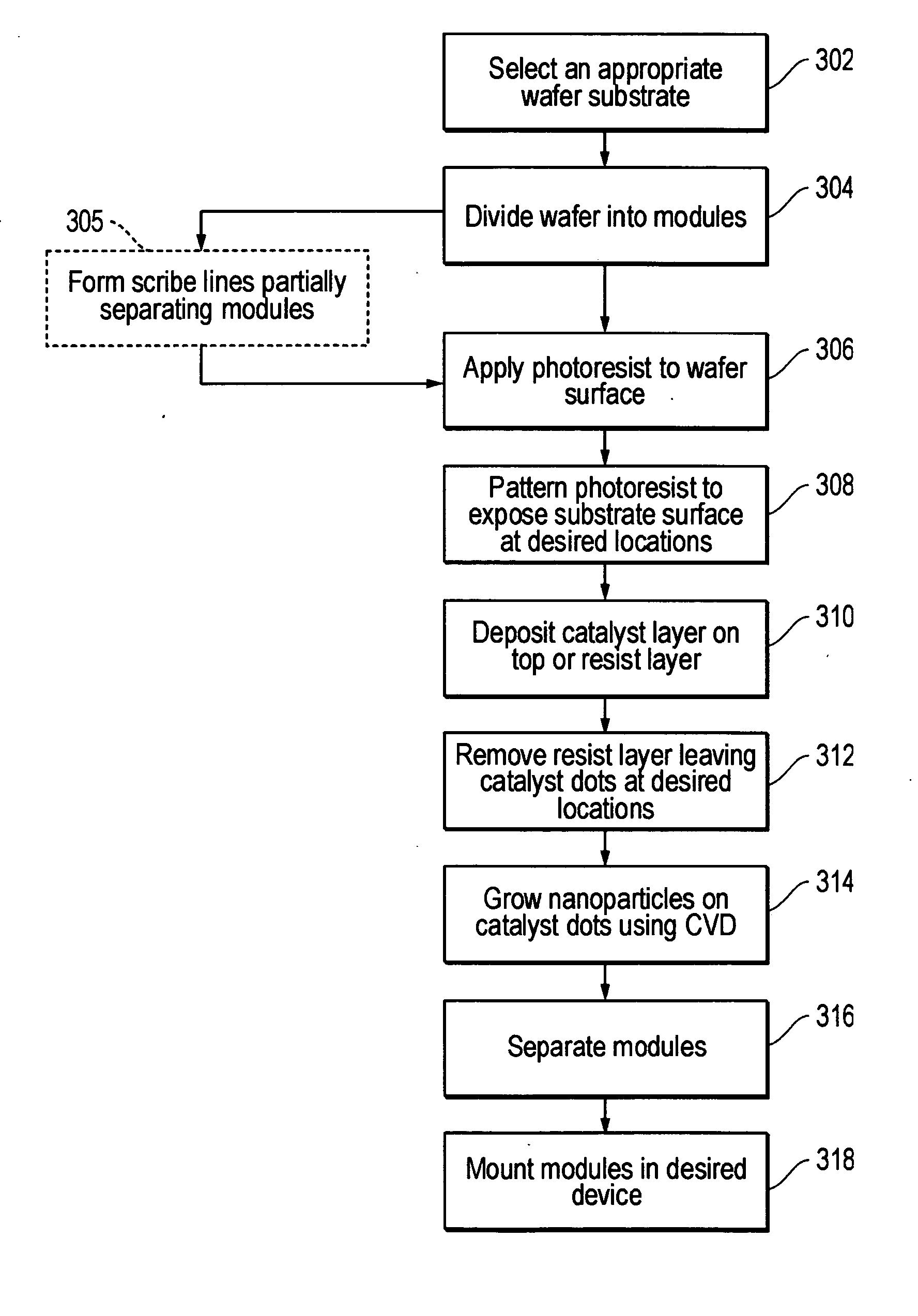
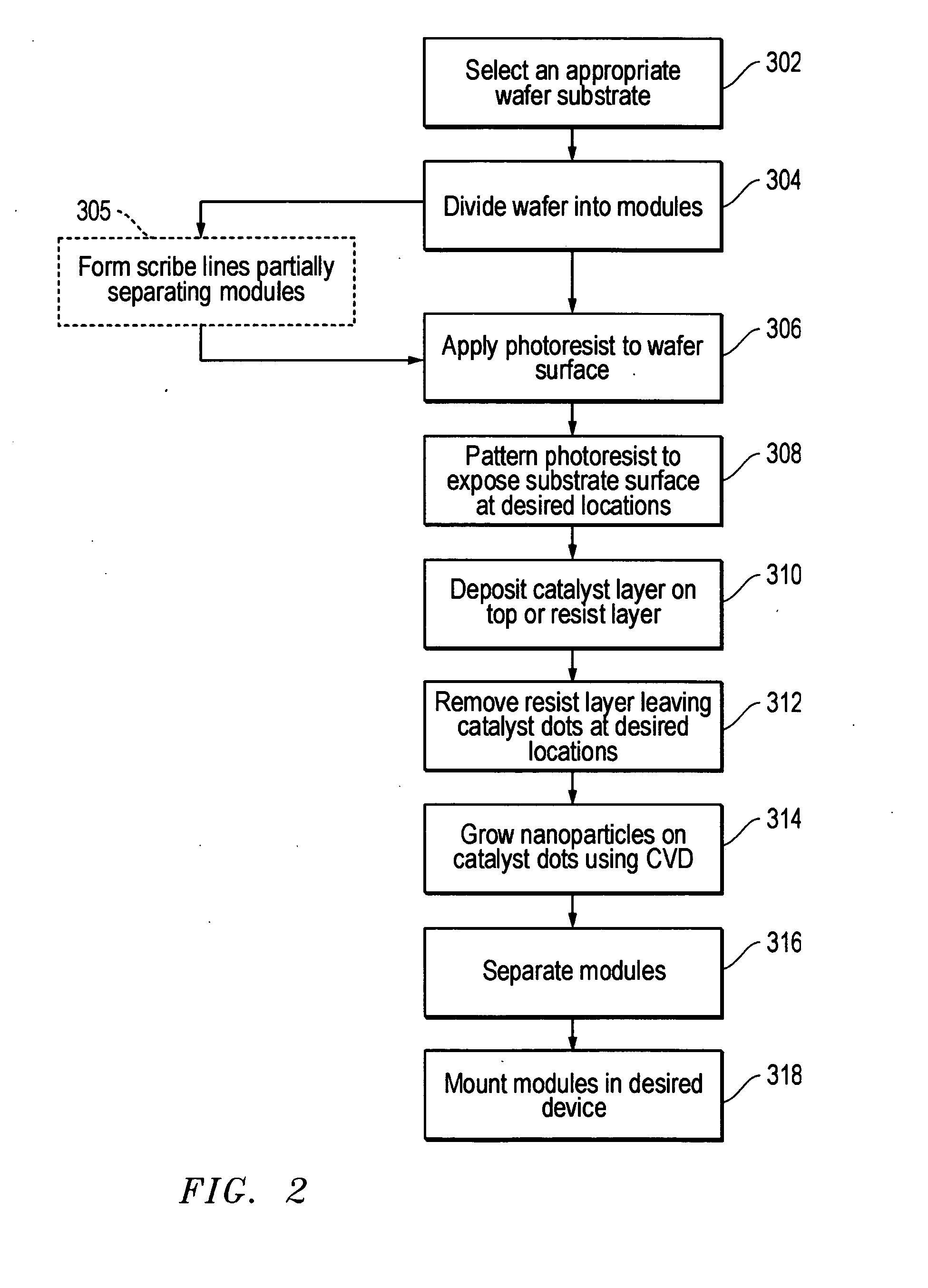
[0032] Preferred embodiments of the present invention are directed to methods and an apparatus for fabricating a batch of nanoparticles or nanodevices using established photolithographic techniques. Nanoparticles can be grown on macroscopic “modules” which can be easily manipulated and shaped to fit standard mounts in various macroscopic devices. A wide variety of electrical and mechanical connections can be incorporated into the macroscopic modules to provide an appropriate interface between various devices and the nanoparticle or nanodevice. Embodiments of the present invention can make use of well-developed techniques to grow nanoparticles, such as a carbon nanotubes, nanowires, quantum dots, or quantum wires, in a defined array on a silicon wafer or other suitable substrate.

[0033] In some embodiments of the invention, photolithographic techniques are used to manufacture the nanoparticle substructure in a manner suitable for large-scale mass production. Photolithography has been...


PUM


Abstract

A method of batch fabrication using established photolithographic techniques allowing nanoparticles or nanodevices to be fabricated and mounted into a macroscopic device in a repeatable, reliable manner suitable for large-scale mass production. Nanoparticles can be grown on macroscopic “modules” which can be easily manipulated and shaped to fit standard mounts in various devices.

Description

[0001] This application claims priority from U.S. Provisional Application No. 60 / 753,561 filed on Dec. 23, 2005, which is hereby incorporated by reference.TECHNICAL FIELD OF THE INVENTION [0002] The present invention relates to nanofabrication and, in particular, to a method of mass-producing nanodevices. BACKGROUND AND SUMMARY OF THE INVENTION [0003] Nanotechnology is commonly defined as the construction and utilization of functional structures with at least one region or characteristic dimension measured in nanometers. Such structures will be hereinafter referred to as nanodevices. The potential applications of nanotechnology are pervasive and the expected impact on society is huge. IC manufacturing technology has already arrived at sub-100 nm technology, while the fabrication of even smaller structures has already been demonstrated on a laboratory scale. [0004] The basic building blocks of nanodevices are nanoparticles or nanostructures, such as carbon nanotubes (CNTs), quantum d...

Claims


Application Information

Patent Timeline
IPC IPC(8): H01L21/00
CPCB82Y15/00B82Y30/00H01J1/304H01J9/025H01J37/06H01J37/073H01J2201/30469H01J2209/0223H01J2237/06341Y10S977/742Y10S977/773Y10S977/752Y10S977/75Y10S977/748Y10S438/962Y10S977/857Y10S977/856Y10S977/745
Inventor SCHWIND, GREGORYMAGERA, GERALDSCIPIONI, LAWRENCE
Owner FEI CO
Why Eureka
Try Eureka