Insulated switching power source device

a power source device and switching technology, applied in the direction of dc-dc conversion, power conversion systems, climate sustainability, etc., can solve the problems of poor transient responsivity, cutoff frequency, deterioration of current transfer rate over time, etc., to avoid the inherent problems of photocouplers, improve the reliability of current transfer rate, and improve the effect of transient responsivity

Inactive Publication Date: 2007-07-05
MURATA MFG CO LTD
View PDF10 Cites 30 Cited by
  • Summary
  • Abstract
  • Description
  • Claims
  • Application Information

AI Technical Summary

Benefits of technology

[0029] With preferred embodiments of the present invention, an automatic control circuit of an insulated type is configured without using a photocoupler, so problems inherent to photocouplers are avoided, and not only are deterioration over time of CRT avoided, but the operating ambient temperature of the insulated switching power source device is set to a wide range. Also, disturbances are responded to by pulse-by-pulse operations, so excellent transient responsivity is achieved.
[0030] Also, the control circuit arranged to control the power switch is provided on the primary side, such that a secondary startup power supply circuit of a separate system is not required as the power transfer transformer. Also, the secondary side only sends timing signals to the primary side, so the signal transfer circuit can be driven at a higher frequency than the switching frequency, enabling simplification of the circuit and reduction in size of components thereof, which is advantageous from the perspective of reduction in the size and the cost of the insulated switching power source device. Also, the design of a switching power source device for fixed switching frequencies if facilitated, since there is no change in switching frequency due to the output state. Also, adding a static deviation reduction circuit as required enables reduction of static deviation beyond that of a hysteresis control switching power source device, and excellent output voltage precision is achieved with switching power source devices for constant voltage output.
[0031] Further, with preferred embodiments of the present invention, properties are achieved in which reverse electric current is suppressed without providing a reverse current suppression circuit of a synchronous rectifier, which is advantageous in reducing the number of components and simplifying the circuit configuration.

Problems solved by technology

The deterioration of CTR (Current Transfer Rate) over time is a problem regarding reliability.
Also, the traditional PWM control used with the Conventional Example 1 has problems of cutoff frequency of the output filter, cutoff frequency of the error amplifier, photocoupler transfer delay, and other problems, and transient responsivity is poor.
Accordingly, there is the problem that the output voltage greatly changes with sudden fluctuations in input voltage and output current.
This circuit that the switching frequency changes according to the state of use, such that designing an insulated switching power source is difficult.
For example, if the switching frequency of the insulated switching power source fluctuates according to the state of use, there are restrictions in the design of the insulated switching power source, and further, main circuit types which can be used are limited.
For example, with a resonance reset forward converter, reduction in frequency generates a surge voltage at the main switch, such that usage thereof is difficult.
The secondary startup power supply circuit is substantially a small-capacity insulated switching power source including a switching device, transformer and other elements, and accordingly is a large and expensive component.

Method used


Image

  • Insulated switching power source device
  • Insulated switching power source device
  • Insulated switching power source device

Examples


first preferred embodiment

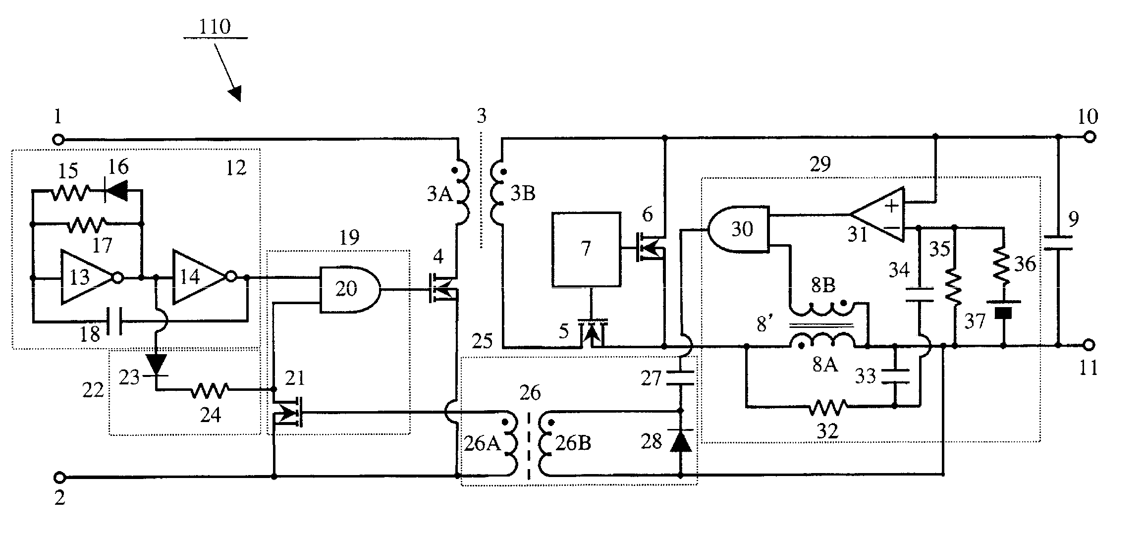
[0046]FIG. 1 illustrates a circuit diagram of a first embodiment of the insulated switching power device of the present invention. An insulated switching power device 110 illustrated in FIG. 1 is a single transistor type resonance reset forward converter. In FIG. 1, the same or equivalent portions as those in FIG. 10 are denoted with the same reference numerals.

[0047] With the insulated switching power device 110 illustrated in FIG. 1, a power transmission transformer 3 includes a primary coil 3A and a secondary coil 3B. One end of the primary coil 3A is connected to a positive-side input terminal 1, and the other end is connected to a negative-side input terminal 2 via a power switch 4 defined by an N-channel MOSFET.

[0048] An oscillation circuit 12 is provided at the primary side of the power transmission transformer 3, and the output thereof is connected to one input of an AND gate 20, and the output of the AND gate 20 is connected to the gate of the power switch 4. A switch dev...

second preferred embodiment

[0082]FIG. 3 illustrates a circuit diagram of a second preferred embodiment of the insulated switching power device according to the present invention. The insulated switching power device 120 illustrated in FIG. 3 is also a single transistor type resonance reset forward converter. In FIG. 3, the same or equivalent portions as those in FIG. 1 are denoted with the same reference numerals, and the description thereof will be omitted.

[0083] The insulated switching power device 120 illustrated in FIG. 3 is different from the insulated switching power device 110 illustrated in FIG. 1 only in that an arrangement is provided in which a resistor 38 is provided serially to the negative-side electric current route, one end of the resistor 38 (the negative-side output terminal 11 side) is connected to the non-inverting input terminal of the comparator 31, and the other end thereof is connected with the reference voltage source 37. Thus, the output electric current is converted into voltage at...

third preferred embodiment

[0086]FIG. 4 illustrates a circuit diagram of a third preferred embodiment of the insulated switching power device according to the present invention. The insulated switching power device 130 illustrated in FIG. 4 is also a single transistor type resonance reset forward converter. In FIG. 4, the same or equivalent portions as those in FIG. 1 or FIG. 10 are denoted with the same reference numerals, and description thereof will be omitted.

[0087] With the insulated switching power device 130 illustrated in FIG. 4, an oscillation circuit 200 is provided at the primary side, and the output thereof is connected to one input of a NOR gate 41, and the output of the NOR gate 41 is connected to the gate of the power switch 4. The switch device 21 including an N-channel MOSFET is connected between the other input of the NOR gate 41 and the negative-side input terminal 2. The NOR gate 41 and the switch device 21 is a power switch on circuit 40 defining a power switch control circuit.

[0088] Th...


PUM


Abstract

A primary side is provided with an oscillation circuit arranged to turn on a power switch at a constant cycle. The secondary side is provided with an on period control circuit arranged to output an off signal for turning the power switch off by detecting output voltage and comparing with a reference triangle wave signal. An insulated signal transfer circuit is provided between the primary side and secondary side to transfer an on signal. The primary side is provided with a power switch off circuit arranged to turn off the power switch based on the on signal.

Description

BACKGROUND OF THE INVENTION [0001] 1. Field of the Invention [0002] The present invention relates to an insulated switching power source device, and particularly to an insulated switching power source device in which a control amount can be transferred from the secondary side to the primary side and direct control can be performed without using a photocoupler, and further which has good transient reactivity. [0003] 2. Description of the Related Art [0004]FIG. 10 illustrates a circuit diagram (Conventional Example 1) of a conventional insulated switching power source device. The Conventional Example 1 is a single transistor type resonance reset forward converter having a fixed voltage output, using a conventional feedback method for the output voltage. [0005] With the insulated switching power source device 100 shown in FIG. 10, a power transfer transformer 3 includes a primary coil 3A and a secondary coil 3B. One end of the primary coil 3A is connected to a positive side input termi...

Claims


Application Information

Patent Timeline
Patent Type & Authority Applications(United States)
IPC IPC(8): H02M3/335
CPCY02B70/1475H02M3/33592Y02B70/10
Inventor MATSUMOTO, TADAHIKO
Owner MURATA MFG CO LTD
Why Eureka
Try Eureka