
Isolator and a modem device using the isolator

Inactive Publication Date: 2007-07-05
HITACHI LTD
View PDF14 Cites 6 Cited by
  • Summary
  • Abstract
  • Description
  • Claims
  • Application Information

AI Technical Summary

Benefits of technology

[0030] Another object of the invention is to miniaturize the communication system and reduce the cost by using the isolator.
[0034] By doing this, it is possible to realize highly dielectric strength by the insulating layer and insulating barrier and to correct a reduction in the signal amplitude due to the stray capacitor by the amplification means, or reduce the degradation of a signal due to crosstalk by synchronizing the operation timing, and realize a compact isolator of high performance and a modem interface circuit.
[0044] The neighborhood of each isolator may be enclosed by a power cable and grounding cable. For example, with respect to the CMOS circuit, there is an advantage that voltage control requiring no control current and a high off-state resistance are obtained. On the other hand, a through phenomenon of the PMOS and NMOS including the parasitic transistor, that is, latch-up is easily generated. However, there is an advantage that by separating the area as mentioned above, such a phenomenon is hardly generated.
[0046] Furthermore, by overlapping electrode areas, connecting the capacities in series, and realizing highly dielectric strength in the horizontal direction, more highly dielectric strength can be realized even if the width of one insulating band cannot be spread due to restrictions on the process. Furthermore, by floating the intermediate electrode during arrangement of the series capacities, extended cables in the strongly energized electric field can be reduced.

Problems solved by technology

However, the aforementioned prior arts do not disclose arts on how capacitive insulating barriers, circuits for using capacitive insulating barriers, arrangement of them, and an insulating method between arranged circuits are structured on a semiconductor substrate and how they are operated so as to realize a monolithic IC isolator, a monolithic IC application circuit, and a monolithic IC line interface circuit.

Method used


Image

  • Isolator and a modem device using the isolator
  • Isolator and a modem device using the isolator
  • Isolator and a modem device using the isolator

Examples


first embodiment

[0157]FIGS. 13a and 13b are respectively the cross sectional view and plane view of monolithic isolators according to the present embodiment. Numerals 901, 902 and 903 in the cross sectional view are respectively a support substrate, a buried oxide film and a silicon layer of an SOI( Silicon On Insulator) substrate. Numeral 904 is a LOCOS( Local Oxidation of Silicon formed by thermal oxidation which is used for element separation such as in CMOS devices.

[0158] Numerals from 921 to 925 are trench insulator films which extend from the surface of the LOCOS to the buried oxide film 902 and are formed in a strip shape, numerals 911 and 912 are respectively primary side and secondary side capacitor electrodes formed respectively by diffusion layers. Numerals 906, 907 and 908 are respectively a first metal layer backing interlayer film, a second metal layer backing interlayer film and a third metal layer backing the interlayer film. Numeral 910 is an intermediate electrode formed with the ...

second embodiment

[0164]FIG. 14a and 14b are respectively cross sectional view and plane view of monolithic isolators according to the present invention. The present embodiment is substantially the same as FIG. 13 embodiment except that (1) the primary side and the secondary side electrodes for the insulator are constituted by third layer metal and the intermediate electrode is constituted the diffusion layer and (2) other than the primary side circuit region and the secondary side circuit region, an independent capacitor region is provided.

[0165] Therefore, only the different points from FIG. 13 embodiment will be explained. Numerals 923, 924, and 964 are trench insulator films which extend from the surface of the LOCOS 904 to the buried oxide film 902 and are formed in a strip shape. Numerals 961 and 962 are respectively capacitor electrodes for the primary side and the secondary side formed by a third layer metal. Numeral 963 is the intermediate electrode formed by a diffusion layer. Numeral 965 i...


PUM


Abstract

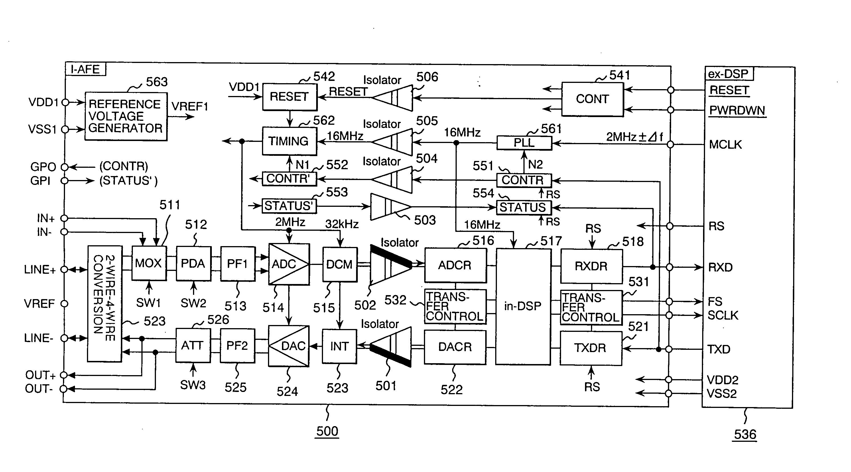
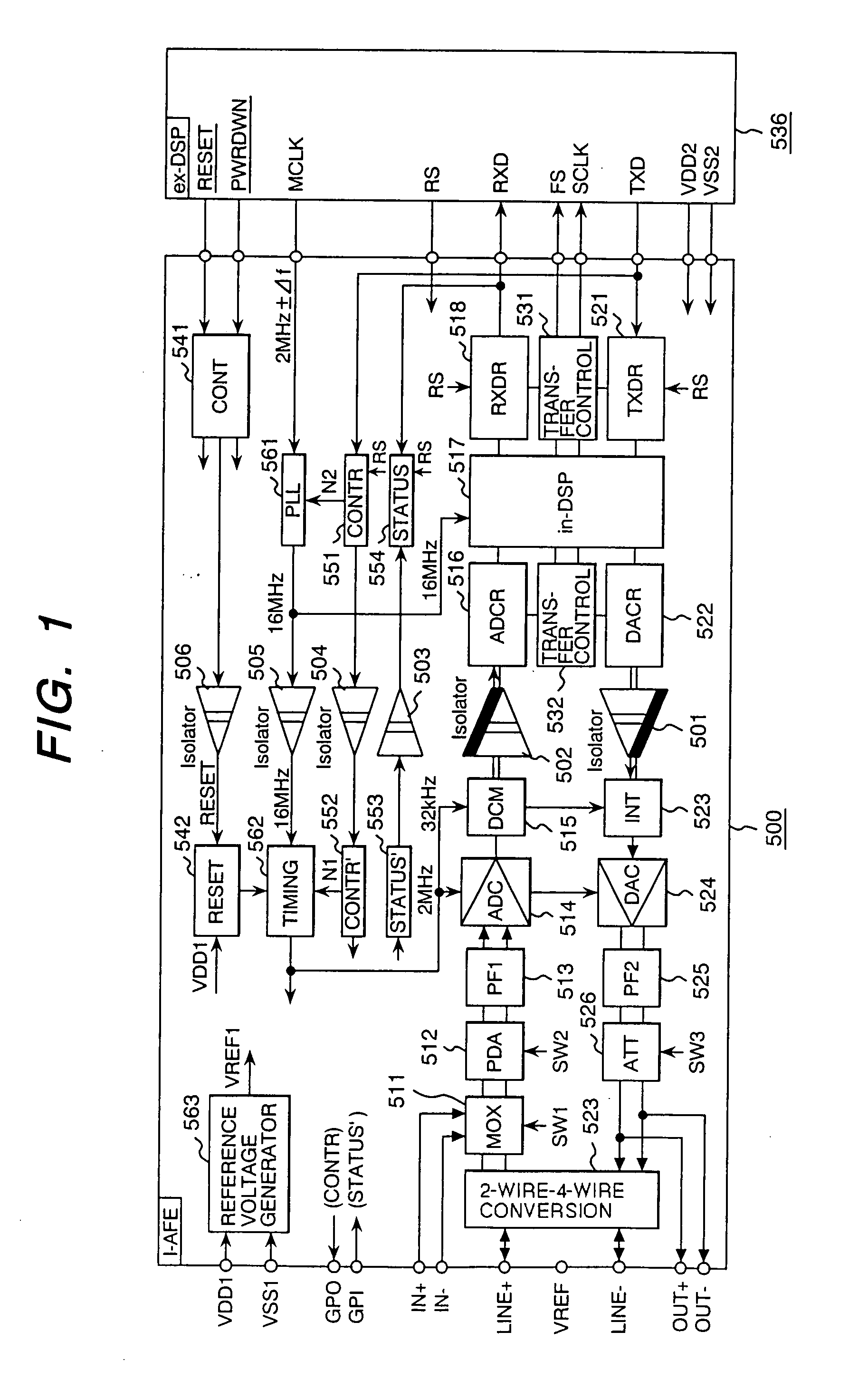
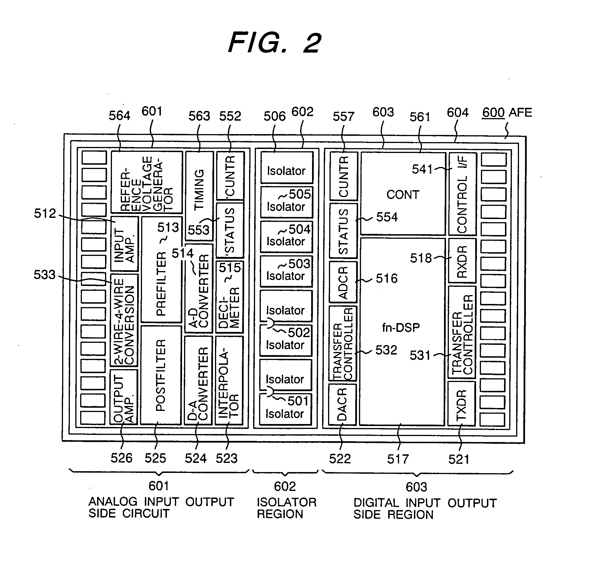
A communication system is provided including a transceiver and an application controller to transmit and receive signals through the transceiver. An isolator which insulates and separates the transceiver and application controller includes primary and secondary side circuits insulated from each other on a substrate and a capacitive insulating means to transfer signals between the primary and second sides while insulating and separating the primary side circuit from the secondary side circuit.

Description

CROSS-REFERENCE TO RELATED APPLICATIONS [0001] This application is a continuation of U.S. application Ser. No. 10 / 377,670, filed Mar. 4, 2003, which, in turn, is a continuation of application Ser. No. 09 / 259,058, filed Feb. 26, 1999 (now U.S. Pat. No. 6,603,807), the entire disclosures of which are hereby incorporated by reference.BACKGROUND OF THE INVENTION [0002] The present invention relates to an isolator used for electrically separating and insulating between circuits and a modem using the isolator. [0003] To protect extremely public network facilities and protect terminals, the communication field requires a high insulation quality for boundaries (hereinafter referred to as line interfaces) between networks and terminals and miniature communication transformers having a high insulation quality have been used. [0004] However, as personal terminals have come into wide use and expanded recently, more miniature and light terminals are required as portable terminals, and a problem ...

Claims


Application Information

Patent Timeline
IPC IPC(8): H04L5/16H04L25/02H04L27/00H04M11/06
CPCH04L25/0266H04L25/0268H04L25/0272H04L25/028H04L25/0292H01L2924/0002H04L27/0002H04M11/06H01L2924/00H04L69/14
Inventor YUKUTAKE, SEIGOHKOJIMA, YASUYUKINEMOTO, MINEHIROAMISHIRO, MASATSUGUIWASAKI, TAKAYUKIMITANI, SHINICHIROFURUKAWA, KATSUHIROKAMADA, CHIYOSHIWATANABE, ATSUOOOUCHI, TAKAYUKIKANEKAWA, NOBUYASU
Owner HITACHI LTD
Learn More