Method for joining electronic parts finished with nickel and electronic parts finished with electroless nickel

a technology of electroless nickel and electronic parts, which is applied in the direction of manufacturing tools, cooking vessels, and so on, can solve the problems of frequent brittle fracture and achieve the effect of preventing brittle fracture and preventing brittle fractur

Inactive Publication Date: 2007-07-12
KOREA ADVANCED INST OF SCI & TECH
View PDF10 Cites 23 Cited by
  • Summary
  • Abstract
  • Description
  • Claims
  • Application Information

AI Technical Summary

Benefits of technology

[0010]An object of the present invention is to provide a method for preventing brittle fracture in a package manufactured by joining an electronic part finished with nickel and an electronic part finished with electroless nickel, more particularly, to a joining method for preventing brittle fracture at a solder joining portion when an electronic part finished with nickel and an electronic part finished with electroless nickel are joined by changing the composition of copper included in the joined solder to control the phase and the spalling phenomenon of intermetallic compounds formed on nickel surface layer and electroless nickel surface layer.

Problems solved by technology

In addition, in case that mechanical impact is applied to a solder joining portion, the brittle fracture frequently occurs near the intermetallic compounds formed at the interface and the reliability depends on formation behaviors of intermetallic compounds and the spalling phenomenon to a large extent.

Method used


Image

  • Method for joining electronic parts finished with nickel and electronic parts finished with electroless nickel
  • Method for joining electronic parts finished with nickel and electronic parts finished with electroless nickel
  • Method for joining electronic parts finished with nickel and electronic parts finished with electroless nickel

Examples


Embodiment Construction

[0038]A better understanding of the present invention may be obtained in light of the following examples which are set forth to illustrate, but are not to be construed to limit the present invention.

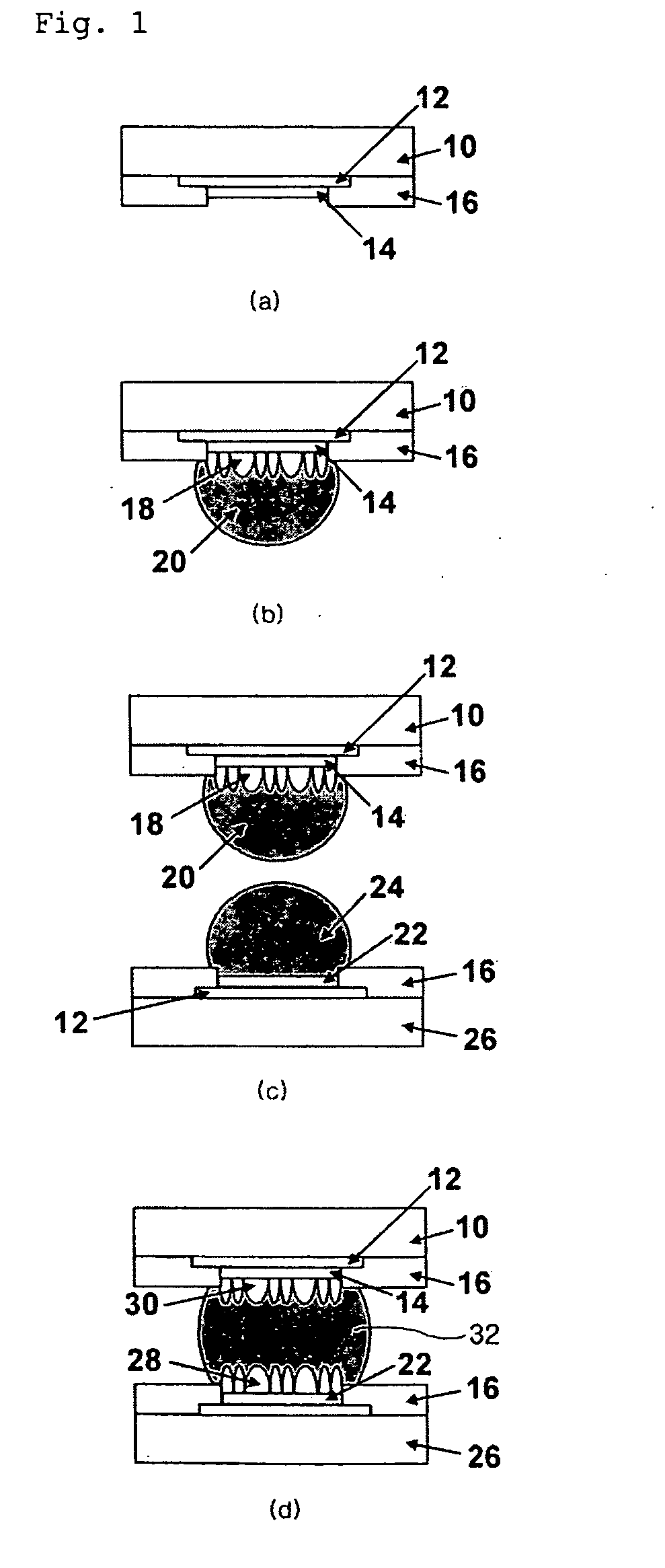
[0039]FIG. 1 is a schematic view showing a process for joining a package part finished with nickel and a printed circuit board finished with electroless Ni(P).

[0040]First, a nickel layer (14) is formed on a metal wiring (12) of a BGA package (10). (FIG. 1(a)) The nickel layer can be deposited by electroplating, sputtering or evaporation method. Meanwhile, one selected from the group consisting of gold, silver, palladium, OSP, tin and tin alloy may be further deposited on a nickel layer with the thickness of 1 μm in order to improve the wettability of nickel with solder and prevent the nickel from being oxidized.

[0041]The lead-free solder (20) of Sn-3.5Ag formed on the nickel layer (14) is reflowed to form an intermetallic compound of Ni3Sn4 (18) to prevent brittle fracture occurring from...


PUM

PropertyMeasurementUnit
thicknessaaaaaaaaaa
compositionaaaaaaaaaa
interconnection densityaaaaaaaaaa

Abstract

The present invention relates, generally, to methods for joining an electronic part finished with nickel and an electronic part finished with electroless nickel, which can prevent a brittle fracture, more particularly, to a method for joining an electronic part finished with nickel and an electronic part finished with electroless nickel with a solder by controlling the composition of the solder to prevent a brittle fracture occurring at the solder joining portion.
A method for joining an electronic part finished with nickel and an electronic part finished with electroless nickel, comprising: (1) reflowing solder to a nickel portion of an electronic part finished with nickel to obtain an electronic part where an intermetallic compound and a solder are formed; (2) obtaining an electronic part finished with an eletroless nickel, of which the nickel portion is connected with the solder; and (3) solder-joining an electronic part finished with nickel obtained in the step (1) and the electronic part finished with electroless nickel obtained in the step (2).

Description

BACKGROUND OF THE INVENTION[0001]1. Field of the Invention[0002]The present invention relates, generally, to methods for joining an electronic part finished with nickel and an electronic part finished with electroless nickel, which can prevent brittle fracture, more particularly, to a method for solder-joining an electronic part finished with nickel and an electronic part finished with electroless nickel by controlling the composition of the solder to prevent brittle fracture occurring at the solder joining portion.[0003]2. Description of the Related Art[0004]As a joining method using solder like flip-chip or BGA package in a package process of an electronic device has a high interconnection density in comparison with a joining method using the existing wire bonding, tape automated bonding (TAB) or lead frame, it has a high efficiency and a short joining distance. Furthermore it loses less electric signals even in a high frequency range, thus it draws an attention as a current and f...

Claims


Application Information

Patent Timeline
Patent Type & Authority Applications(United States)
IPC IPC(8): A47J36/02
CPCB23K35/262H01L24/10H01L24/13H01L2924/014H01L2924/0105H01L2924/01047H01L2924/01033H01L24/81H01L2224/13139H01L2224/16H01L2224/81193H01L2224/8121H01L2224/81815H01L2924/01013H01L2924/01015H01L2924/01022H01L2924/01029H01L2924/0103H01L2924/01046H01L2924/01051H01L2924/01074H01L2924/01078H01L2924/01079H01L2924/01082H01L2924/01327H05K3/244H05K3/3463H05K2203/072H01L2924/00013H01L2924/01005H01L2924/01006H01L2924/01023H01L2924/01024H01L2924/00014H01L2224/13099H01L2924/00H01L2224/13B64F5/40
Inventor SON, YOON-CHULKIM, JONG-YEONYU, JIN
Owner KOREA ADVANCED INST OF SCI & TECH
Why Eureka
Try Eureka