Method of microminiaturizing a nano-structure

a nano-structure and micro-miniaturization technology, applied in the field of nano-structure fabrication, can solve the problems of increasing switching speed, reducing the size of all nano-devices and nano-components, and achieving the effect of more miniaturization

Inactive Publication Date: 2007-07-12
LIN MING NUNG
View PDF19 Cites 7 Cited by
  • Summary
  • Abstract
  • Description
  • Claims
  • Application Information

AI Technical Summary

Problems solved by technology

In electronics, only few electrons instead of thousands of electrons can operate the SET (Single Electron Transistor) and spin-valve through nano-structure; thus, it not only decreases the energy and power consumption but also increases the switching speed.
However, the size of all the nano-devices and nano-components reduces to some degree, the fundamental physical limit will restrict the fabricating capability in smaller nano-structure, so that it can not breakthrough towards more miniaturizing.
Therefore, how to breakthrough this bottleneck such that making the nano-scale of nano-aperture 3 be smaller becomes the impending crucial technical tough question of all experts in various fields; The solution being subject to the industrial practical feasibility in mass production and cost-effective economical principle so that the choice of means in technical breakthrough becomes more difficult;
The scientists who understand the nano-science and the experts who familiarize with nano-technology are all aware of the benefits of working out the devices being smaller than 50 nm or even 1˜2 nm, but none of better solution or effective technical breakthrough is proposed, announced or applied.

Method used


Image

  • Method of microminiaturizing a nano-structure
  • Method of microminiaturizing a nano-structure
  • Method of microminiaturizing a nano-structure

Examples


second embodiment

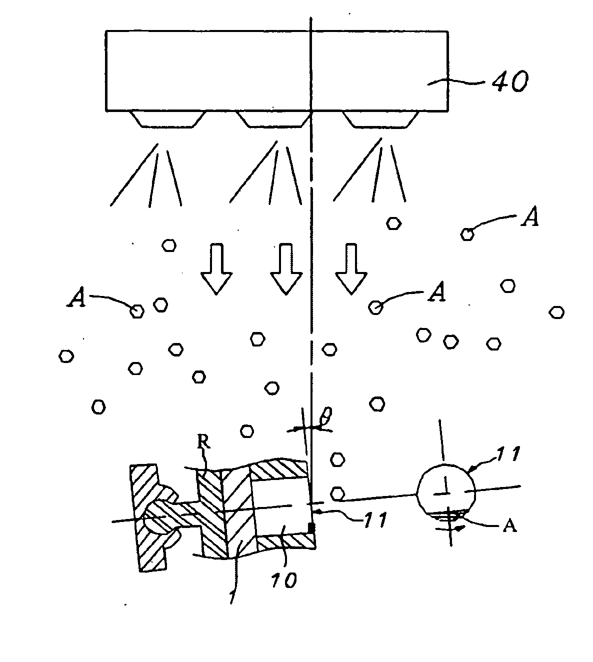
[0079] As shown in the FIG. 17 is the present invention in fabricating a nano rod 60 in more microminiaturizing manner.

[0080] In this fabricating process, the substrate 1 is firmly placed on the rotary console P with capability of 2-D leftwards and rightwards tilt and one-by-one orderly adjust the leftwards and rightwards tilt angle θ of said rotary console P as θ1, θ2 and θ3 etc. (as shown in f, g, h, i view of the FIG. 17 and each of corresponding top view);

[0081] Thereby the deposit material B of molecule or atom state passing through said reduced nano-aperture 20 will one-by-one continuously form a nano rod 60, whose width being smaller than that of the orifice diameter in nano cylindrical pore 10, on the surface of said substrate 1 (as shown in j view of the FIG. 17 and corresponding top view);

[0082] Therefore, the structure of said nano rod 60 is a bulged rod, which is formed on said substrate 1 by deposition of said deposit material B of molecule or atom state through one-b...

third embodiment

[0083] As shown in the FIG. 18 is the present invention in fabricating a nano ring 70 in more microminiaturizing manner.

[0084] In this fabricating process, the substrate 1 is firmly placed on the tilt-rotary console R with capability of 3-D tilt and rotation and one-by-one orderly adjust said the rotation angle Φ of said tilt-rotary console R as Φ1, Φ2, Φ3 and Φ4 etc. as well as in coordination with forwards and backwards tilt angle θ plus leftwards and rightwards yaw angle θ as θ4, θ5, θ6 and θ7 etc. (as shown in m, n, o, p, q, r, s view of the FIG. 18 and each of corresponding top view);

[0085] Thereby the deposit material B of molecule or atom state passing through said reduced nano-aperture 20 will one-by-one continuously form a nano ring 70, whose size being smaller than that of the orifice diameter in nano cylindrical pore 10, on said substrate 1 (as shown in s view of the FIG. 18 and corresponding top view);

[0086] Therefore, the structure of said nano ring 70 is a bulged rin...

fourth embodiment

[0087] As shown in the FIG. 19 through FIG. 22 is the present invention in fabricating a nano structure with closed top on the nano cylindrical pore 80, which is existing pattern formed on said photo-resist 2 of said substrate 1 (as shown in the FIG. 19).

[0088] The fabricating process steps comprise:

[0089] (a): By means of etching from solution or sputtering from high energy gas particle, first drill a nano orifice 81 on the top of nano cylindrical pore 80 with closed top (as shown in the FIG. 20);

[0090] (b): Directly pass the deposit material B of gas molecule or atom state through the nano orifice 81 (as shown in the FIG. 21); Thereby the nano quantum dot 90 with same nano-scale as the orifice diameter of said nano orifice 81 is directly formed on said substrate 1, which being laid beneath the bottom of said nano cylindrical pore 80 (as shown in a, b, c and view of the FIG. 22); and

[0091] (c):By means of solution rinsing (i.e. wet etching) or gas etching (i.e. dry etching), rem...


PUM

PropertyMeasurementUnit
physical sizeaaaaaaaaaa
sizeaaaaaaaaaa
orifice diameteraaaaaaaaaa

Abstract

The present invention provides a “microminiaturizing method of nano-structure” with fabricating process steps as follows: First deposit the material of molecule or atom state on the top-opening of the nano cylindrical pore, which having formed on the substrate, so that the diameter of said top-opening gradually reduce to become a reduced nano-aperture, whose opening diameter is smaller than that of said top-opening; Then, directly pass the deposit material of gas molecule or atom state through said reduced nano-aperture; thereby a nano-structure of nano quantum dot, nano rod or nano ring with smaller nano scale is directly formed on the surface of said substrate, which being laid beneath the bottom of said nano cylindrical pore.

Description

[0001] This application claims the benefit of provisional U.S. Patent Application Ser. No. 754,614, filed Dec. 30, 2005.FIELD OF THE PRESENT INVENTION [0002] The present invention relates to the fabrication of nano-structure in more microminiaturizing manner, particularly provides an advanced microminiaturizing method in connection with the nano scale in existing variety of nano-structure and nano-device; [0003] Especially, by directly using the current fabricating facilities, it fabricates out nano-structure of nano-quantum-dot in smaller manner, nano-rod in thinner manner and nano-ing in narrower manner than the minimum nano scale limit of the current fabricating facilities. BACKGROUND OF THE PRESENT INVENTION [0004] The development of the nano-science nowadays has been extensively applied in a variety of fields, especially in the semiconductor industry, which constantly produces many nano-devices and nano-components, such as: [0005] In electronics, only few electrons instead of t...

Claims


Application Information

Patent Timeline
Patent Type & Authority Applications(United States)
IPC IPC(8): H01L21/44
CPCB81C99/0085B82Y10/00B82Y15/00H01L29/66439H01L21/76838H01L29/127B82Y30/00B82B3/00B82B1/00H01L21/44B82Y40/00
Inventor LIN, MING -NUNG
Owner LIN MING NUNG
Why Eureka
Try Eureka