

Ingaas/gaas lasers on-silicon produced by-lepecvd and mocvd
a technology of gaas lasers and silicon, which is applied in the direction of laser details, nanooptics, semiconductor devices, etc., can solve the problems of reducing the performance of gaas lasers, requiring high substrate temperatures for gaas lasers to be grown, and reducing the speed of gaas lasers, etc., to achieve the effect of improving the surface roughness of gaas, reducing the cost of gaa
- Summary
- Abstract
- Description
- Claims
- Application Information
AI Technical Summary
Benefits of technology
Problems solved by technology
Method used
Image

Examples
first embodiment
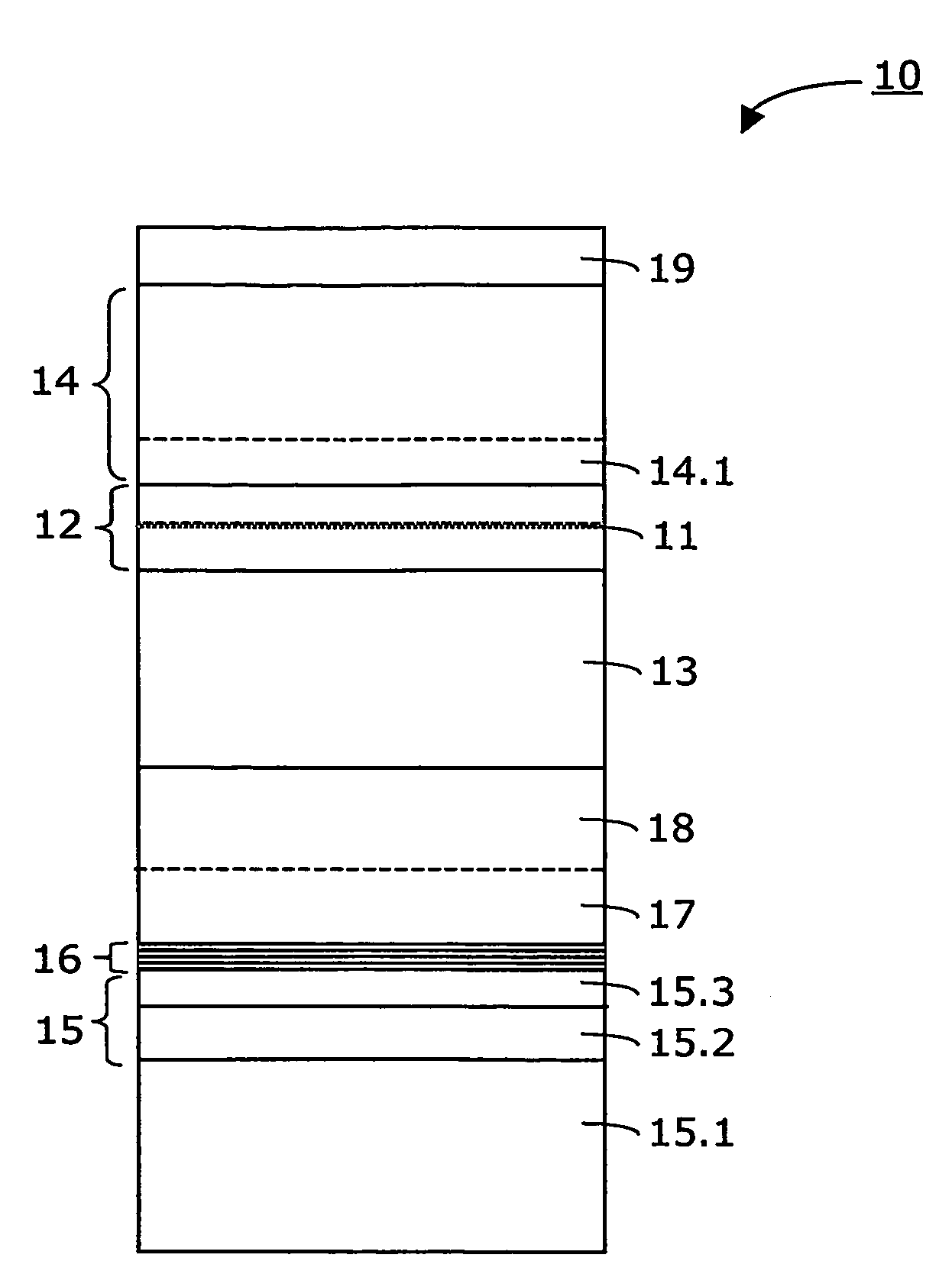
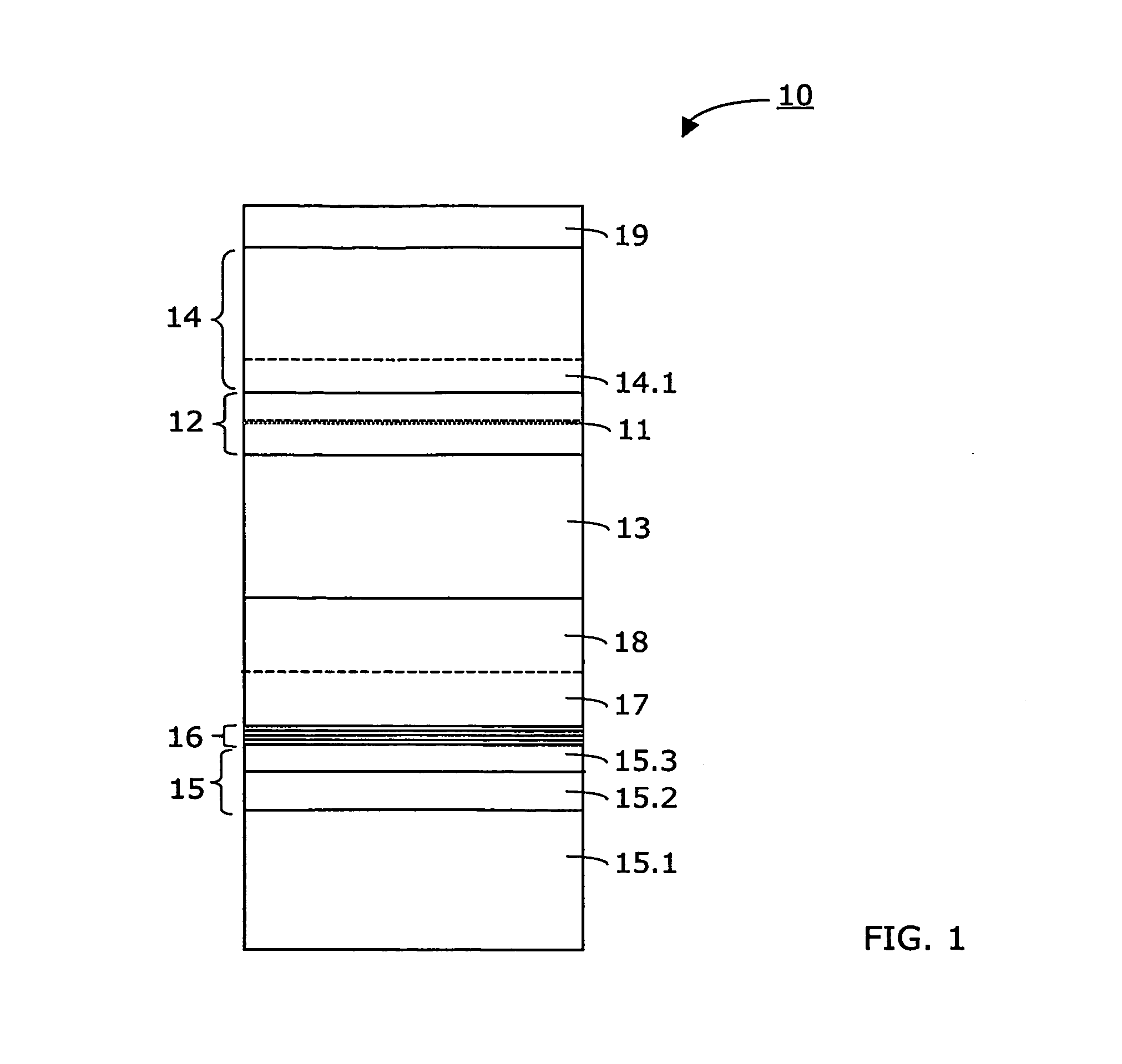
[0034] Further details of a first embodiment is given in the following table:
ReferenceNumberTypicalof LayerMaterialDopingThickness RangeThickness15.1Si-wafer—100-1000μm˜200μm[001]-oriented, 6afterdegree offpolishing15.2SiGe (graded)—0.3-14μm˜5μm15.3Ge (pure)—0.5-5μm1μm16As / Gadoped or1-3nm2nmundoped17GaAsdoped or0.2-2μm˜0.7μmundoped18GaAsn+-doped,0.2-2μm˜0.7μmSi 7 · 1018 cm−313Al0.35Ga0.65Asn-doped,1-5μm˜2μmSi 2 · 1018 cm−312GaAsundoped0.2-0.4μm˜0.29μm11InGaAs (strained)—5-15nm˜10nmIn concentrationbetween 20-25%14.1Al0.35Ga0.65Asundoped0.1-0.3μm˜0.2μm14Al0.35Ga0.65Asp-doped,1-5μm˜2μmZn 5 · 1017 cm−319GaAsP++-doped,0.1-0.3μm˜0.15μmZn 1 · 1019 cm−3
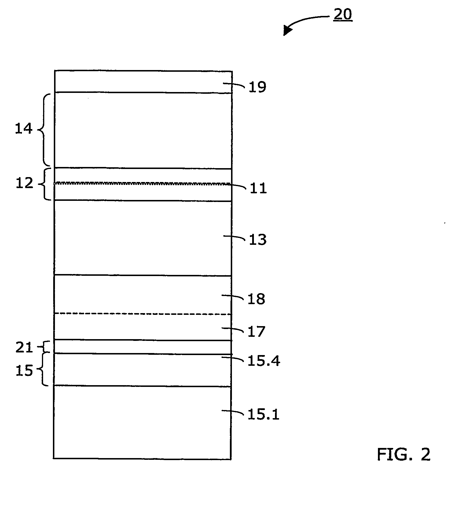
[0035] Another laser structure 20, according to the present invention, is depicted in FIG. 2. The corresponding details are given in the following table:
ReferenceNumberTypicalof LayerMaterialDopingThickness RangeThickness15.1Si-wafer—100-1000μm˜300μmafterpolishing15.4Ge (pure)—0.5-5μm˜2μm21GaAs (formed atdoped or1-3nm2nmTs1)undoped17GaAs (f...
second embodiment
[0044] As stated in connection with the second embodiment, the virtual Germanium substrate 15 may comprise a pure Germanium layer 15.4 being formed directly on the Silicon substrate 15.1. The pure Germanium layer 15.4 has a thickness between 0.5 μm and 5 μm, and preferably between 1 μm and 2 μm.
[0045] Preferably, the second Gallium Arsenide waveguide layer 17 is undoped and has a thickness between 0.2-2 μm. It may have a thickness of about 1 μm, for instance.
[0046] The Gallium Arsenide waveguide layer 12 may be undoped. It has a thickness between 0.2-0.4 μm, and preferably about 0.29 μm.
[0047] Several metal organic chemical vapour deposition process steps are carried out when forming the active laser structure. Advantageous results are achieved if the active laser structure comprises an InGaAs quantum well laser structure. Preferably, the active laser structure comprises an InGaAs / AlGaAs / GaAs quantum well laser structure with a compressively strained InGaAs quantum well 11.
[0048]...
PUM
| Property | Measurement | Unit |
|---|---|---|
| thickness | aaaaa | aaaaa |
| thickness | aaaaa | aaaaa |
| thickness | aaaaa | aaaaa |
Abstract
Description
Claims
Application Information