Plasma doping method

a technology of plasma and doping method, which is applied in the direction of individual semiconductor device testing, semiconductor/solid-state device testing/measurement, instruments, etc., can solve the problems of large number of ions being lost, the dose control method for controlling the element characteristics has not been developed, and the beam transportation itself becomes difficult. , to achieve the effect of high accuracy, accurate control of impurity doping amount, and stable control

Inactive Publication Date: 2007-07-19
PANASONIC CORP
View PDF25 Cites 24 Cited by
  • Summary
  • Abstract
  • Description
  • Claims
  • Application Information

AI Technical Summary

Benefits of technology

[0016] It is another object of the invention to provide a plasma doping method that can realize high in-plane uniformity of a dose and can control the dose with high accuracy.
[0061] Further, it is possible to form the impurity region having excellent in-plane uniformity.

Problems solved by technology

As a result, the ion beam may collide against the inner wall of a beam line, and a large number of ions may be lost.
For example, when B+ ions are implanted, if the acceleration energy becomes 2 keV or less, the throughput starts to be lowered, if the acceleration energy becomes 0.5 keV or less, the beam transportation itself become difficult.
However, a dose control method for controlling the element characteristics has not been developed yet.
Up to now, a method for changing the dose by way of changing a plasma doping time has been tested, but this method does not obtain sufficient control precision, and as a result, it is unpractical.
In particular, while there is a recent progress in a large diameter of a wafer, it is very difficult to obtain a uniform dose in the surface.

Method used


Image

  • Plasma doping method
  • Plasma doping method
  • Plasma doping method

Examples


first embodiment

[0073] Hereinafter, a first embodiment of the invention will be described in detail with reference to the drawings.

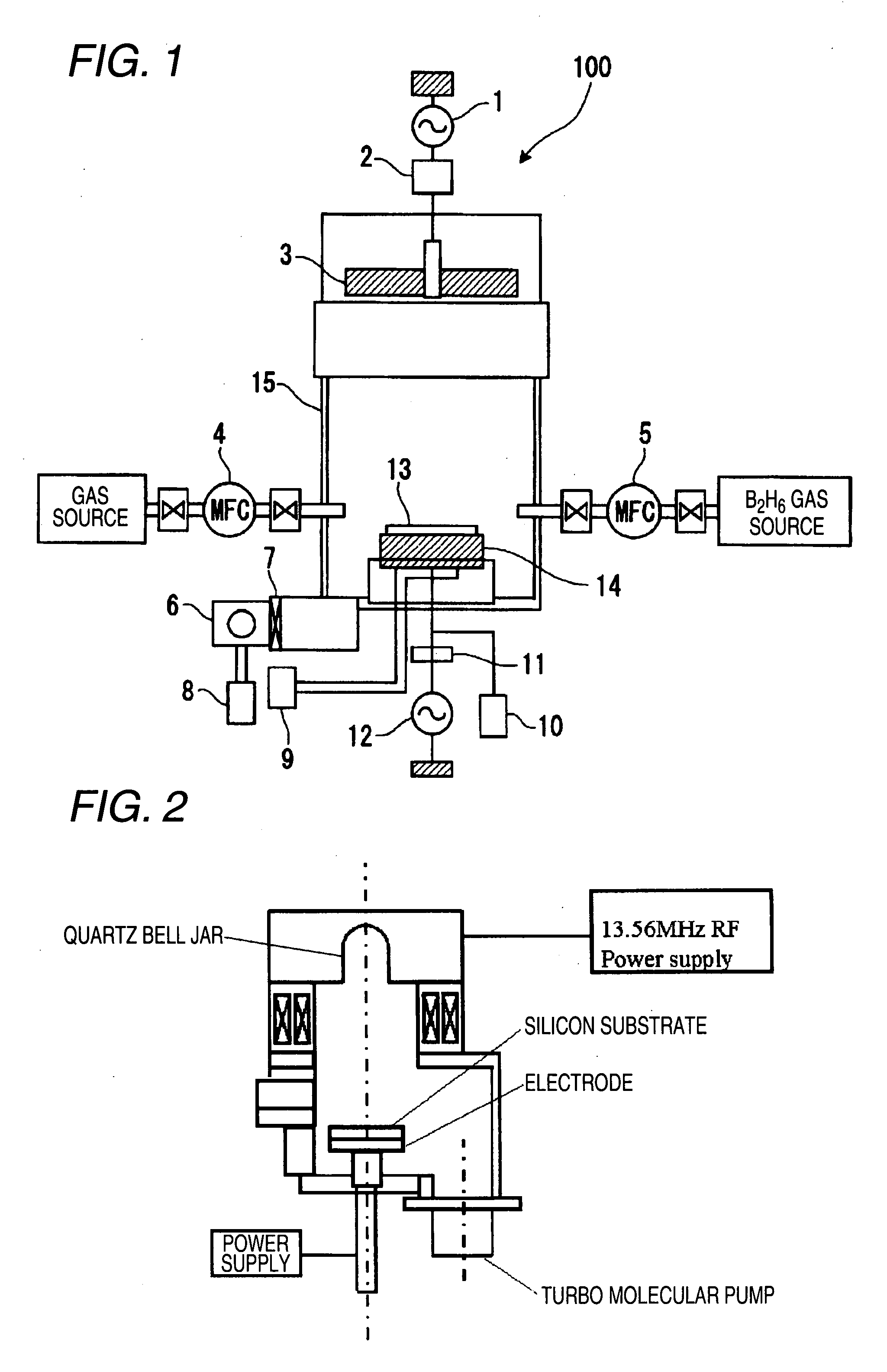
[0074] An apparatus shown in FIG. 1 is referred to as a plasma doping apparatus A (PD apparatus A).

[0075] In this embodiment, upon doping of an impurity, a concentration of gas plasma containing impurity ions to be doped is set such that doping of the impurity ions and sputtering of a surface of a silicon substrate (silicon wafer) are saturated. According to this, a dose can be accurately controlled without depending on a time variation. Therefore, it is possible to form an impurity region in which an impurity concentration is stably controlled with high accuracy. Further, it is possible to form an impurity region having excellent in-plane uniformity.

[0076] Here, the concentration of the gas plasma is set such that doping of the impurity ions and sputtering of the surface of the substrate are saturated. According to this, the dose can be accurately controlled without...

second embodiment

[0087] Hereinafter, a second embodiment of the invention will be described with reference to FIG. 2.

[0088] An apparatus shown in FIG. 2 is referred to as a plasma doping apparatus B (PD apparatus B).

[0089]FIG. 2 is a schematic plan view of an impurity doping apparatus used in the second embodiment of the invention. In FIG. 2, the impurity doping apparatus uses a helicon plasma device, and thus, in this device, B2H6 / He gas and He gas are supplied through mass flow controllers 24 and 25.

[0090] Here, the impurity is also doped into a silicon substrate (sample) 33 placed on a sample table 34 in a reaction chamber 35. High frequency is supplied to a coil 23 by a high-frequency power supply 21, and then the B2H6 / He gas and He gas to be supplied through the mass flow controllers 24 and 25 are plasmized.

[0091] In this apparatus, the mass flow controllers 24 and 25 are controlled with high accuracy, and the mixture ratio of B2H6 / He is controlled. Accordingly, the concentration of the gas...

example 1

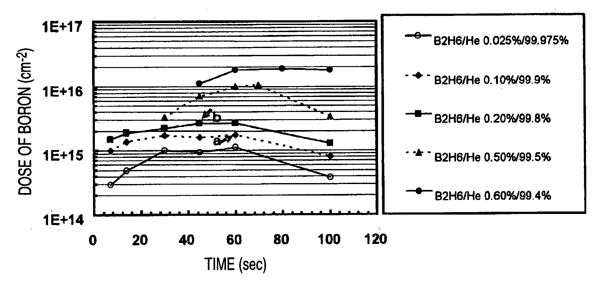
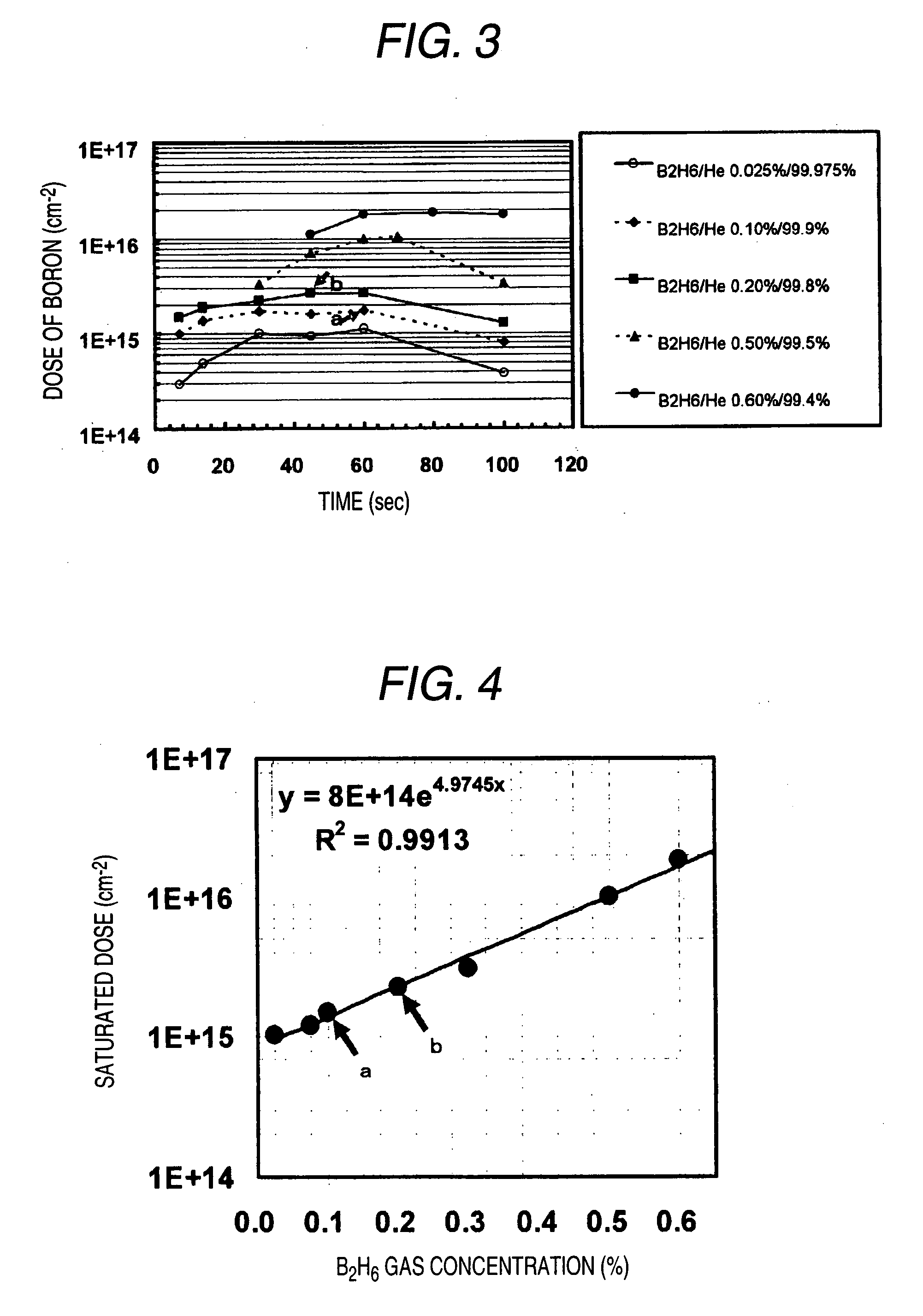
[0092] Plasma doping is performed on a 200 mm substrate using the PD apparatus B described in the second embodiment with reference to FIG. 2 while the dose of boron and the plasma doping time are changed.

[0093]FIG. 3 shows the measurement result of the relationship between the dose of boron and the plasma doping time at this time. The vertical axis represents the dose and the horizontal axis represents the plasma doping time.

[0094] If a bias is applied by irradiating the mixture gas plasma of B2H6 and He (B2H6 / He plasma) onto the silicon substrate, there is a time when doping and sputtering of boron are saturated (balanced). Further, in this embodiment, it can be seen that the saturation time is comparatively long and ease to stably use. That is, if plasma irradiation starts, a dose is initially increased, but a time at which the dose is made substantially uniform without depending on a time variation is continued. In addition, if the time is further increased, the dose is decreas...


PUM


Abstract

A plasma doping method that can control a dose precisely is realized. In-plane uniformity of the dose is improved. It has been found that, if a bias is applied by irradiating B2H6 / He plasma onto a silicon substrate, there is a time at which a dose of boron is made substantially uniform, and the saturation time is comparatively long and ease to stably use, compared with a time at which repeatability of an apparatus control can be secured. The invention has been finalized focusing on the result. That is, if plasma irradiation starts, a dose is initially increased, but a time at which the dose is made substantially uniform without depending on a time variation is continued. In addition, if the time is further increased, the dose is decreased. The dose can be accurately controlled through a process window of the time at which the dose is made substantially uniform without depending on the time variation.

Description

BACKGROUND OF THE INVENTION [0001] 1. Background of the Invention [0002] The present invention relates to a plasma doping method, and in particular, to a plasma doping method for doping an impurity into a surface of a solid sample such as a semiconductor substrate. [0003] 2. Description of the Related Art [0004] As a technology for doping an impurity into a surface of a solid sample, a plasma doping (PD) method for ionizing the impurity and doping the ionized impurity into a solid at low energy is well known (for example, see U.S. Pat. No. 4,912,065). [0005] On the other hands, among the methods for doping an impurity, an ion implantation method is most widely used at present. The plasma doping method is described in “Column of Shallow Junction Ion Doping of FIG. 30 of Front End Process in International Technology Roadmap for Semiconductors 2001 Edition (ITRS2001)” and “International Technology Roadmap for Semiconductors 2003 Edition (ITRS2003)” as a next-generation technology for i...

Claims


Application Information

Patent Timeline
Patent Type & Authority Applications(United States)
IPC IPC(8): H01L21/66H01L21/04G01R31/26
CPCH01J37/32412H01L29/66795H01L21/2236H01L21/265
Inventor SASAKI, YUICHIROOKASHITA, KATSUMIITO, HIROYUKIMIZUNO, BUNJIOKUMURA, TOMOHIRO
Owner PANASONIC CORP
Why Eureka
Try Eureka