

Process for producing thin photosensitized semiconducting films
a semiconducting film and photoensitization technology, applied in the direction of light-sensitive devices, solid-state devices, electrolytic capacitors, etc., can solve the problem of difficult photoensitization of thin films obtained with chromophores, and achieve satisfactory adhesion to a support, the effect of reducing the difficulty of photoensitization
- Summary
- Abstract
- Description
- Claims
- Application Information
AI Technical Summary
Benefits of technology
Problems solved by technology
Method used
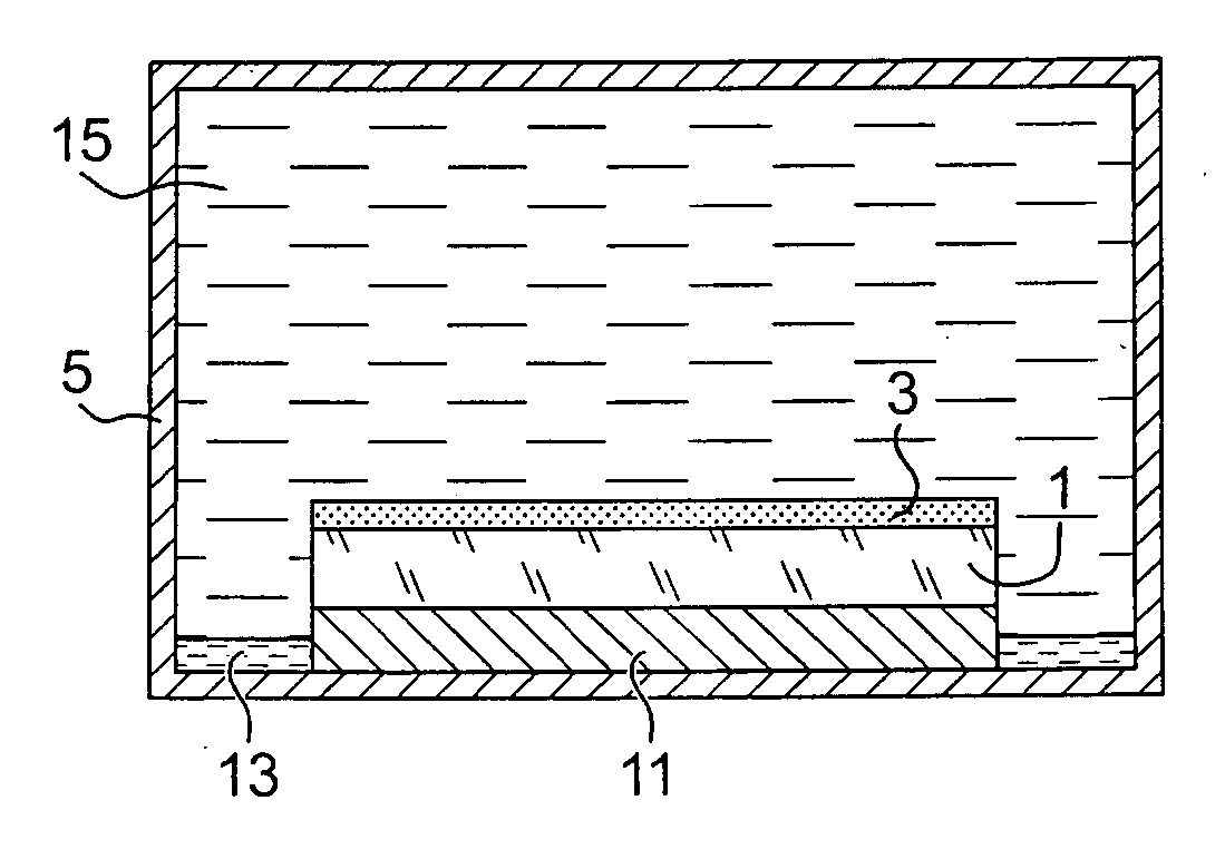
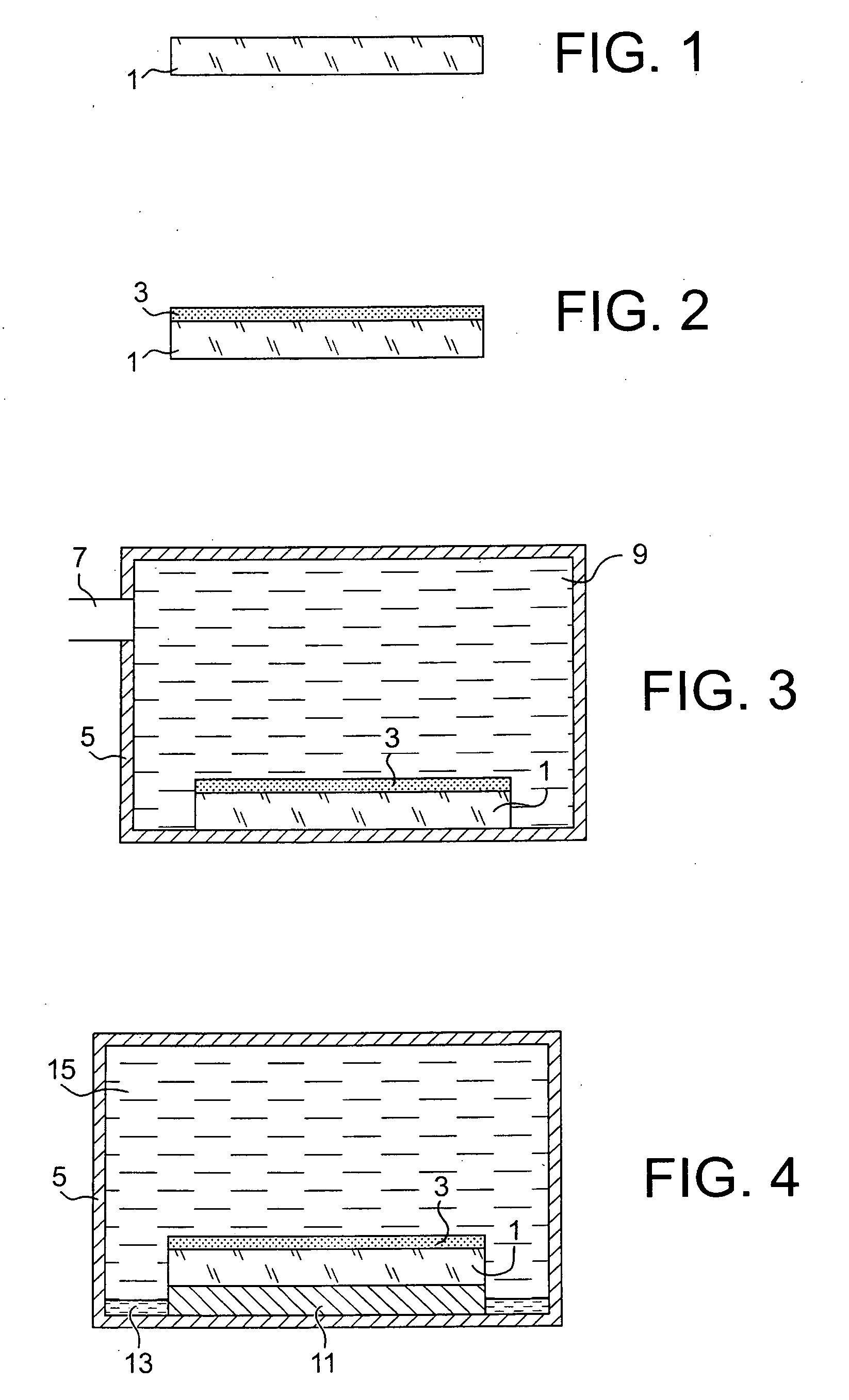
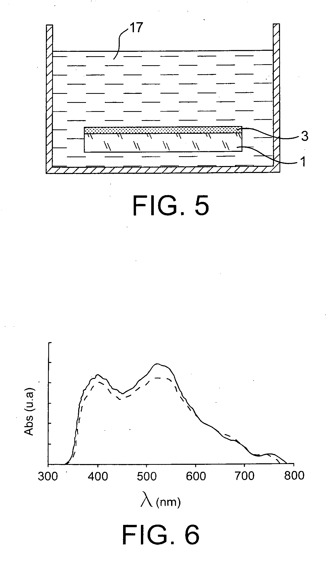
Image

Examples
Embodiment Construction
[0081] The invention will now be described with regard to the following exemplary embodiment.
a) Preparation of the Support
[0082] Within the context of this example, the transparent support was a rectangular (1×5 cm) support made of borosilicate glass (type BK-7 manufactured by the company Schott) with a thickness of 2 mm. The refractive index was 1.52 at a wavelength of 600 nm. It was neither coated with a transparent conducting film nor with any dense semiconducting film so as to eliminate the optical perturbations induced by their presence on the surface on the support. The transparent support was firstly cleaned according to the following procedure. The cleaning of the surface is intended to be coated was carried out with a dilute (1 vol %) hydrofluoric acid solution. Next, this surface was rinsed with deionized pure water and cleaned using a detergent solution of vegetable soap (called “Green Soap”, from Eli Lilly Co.). Finally this surface was rinsed with deionized pure wate...
PUM
 Abstract
Description
Claims
Application Information