Light emitting element, light emitting device, and electronic device

a technology light emitting devices, which is applied in the direction of discharge tube luminescnet screens, other domestic articles, natural mineral layered products, etc., can solve the problems of high cost, short circuits that are easy to occur, and the number of malfunctions of light emitting elements cannot be reduced sufficiently, so as to reduce malfunctions, increase lifetime, and reduce driving voltage

Inactive Publication Date: 2007-07-26
SEMICON ENERGY LAB CO LTD
View PDF10 Cites 56 Cited by
  • Summary
  • Abstract
  • Description
  • Claims
  • Application Information

AI Technical Summary

Benefits of technology

[0008] It is an object of the present invention to provide a light emitting element which can reduce malfunctions due to oxidation or crystallization of a compound. Further, it is an object of the present invention to provide a light emitting element which has a low driving voltage and which can increase lifetime longer than a conventional light emitting element.
[0015] Since “the layer containing the carbazole derivative represented by General Formula (1) and the substance having an electron accepting property with respect to the carbazole derivative represented by General Formula (1)” has a function of generating holes, carrier density is increased. Since conductivity- is improved as the result, there are few changes in driving voltage depending on a thickness of “the layer containing the carbazole derivative represented by General Formula (1) and the substance having an electron accepting property with respect to the carbazole derivative represented by General Formula (1)”. Therefore, by changing the thickness of “the layer containing the carbazole derivative represented by General Formula (1) and the substance having an electron accepting property with respect to the carbazole derivative represented by General Formula (1)”, a distance between the layer containing a light emitting substance and the first or second electrode can be easily adjusted.
[0016] In other words, a length of light path through which emitted light passes (light path length) can be easily adjusted in order to be a length capable of efficiently extracting light outward or improving color purity of light extracted outward. In addition, by thickening “the layer containing the carbazole derivative represented by General Formula (1) and the substance having an electron accepting property with respect to the carbazole derivative represented by General Formula (1)”, an asperity on a surface of the first electrode can be reduced, and a short circuit between the electrodes can be easily prevented.
[0036] In the light emitting element of the present invention, by forming at least one layer of the plurality of layers between the first and second electrodes using the layer containing the carbazole derivative represented by General Formula (1) and the substance having an electron accepting property with respect to the carbazole derivative represented by General Formula (1), a problem of causing malfunctions of the light emitting element due to crystallization, which is generated when an anode is made from metal oxide, can be solved and driving voltage can be reduced.
[0037] In the light emitting element of the present invention, since electron transfer is performed even before the application of voltage to “the layer containing the carbazole derivative represented by General Formula (1) and the substance having an electron accepting property with respect to the carbazole derivative represented by General Formula (1)”, “the layer containing the carbazole derivative represented by General Formula (1) and the substance having an electron accepting property with respect to the carbazole derivative represented by General Formula (1)” becomes a film having an extremely high conductivity. Therefore, it is possible to provide an electroluminescent element with low driving voltage and low power consumption.
[0039] Therefore, “the layer containing the carbazole derivative represented by General Formula (1) and the substance having an electron accepting property with respect to the carbazole derivative represented by General Formula (1)” can be prevented from short circuits because the layer can be thickened without increasing voltage, and optical design can be optimized. Accordingly, a highly reliable electroluminescent element with high light emitting efficiency can be provided.

Problems solved by technology

However, since molybdenum oxide is easy to be crystallized, the number of malfunctions of the light emitting element due to the crystallization cannot be reduced sufficiently.
In other words, since molybdenum oxide is crystallized to form a projection portion and loses flatness, a short circuit easily occurs and there is a problem of easily causing malfunctions of the light emitting element.

Method used


Image

  • Light emitting element, light emitting device, and electronic device
  • Light emitting element, light emitting device, and electronic device
  • Light emitting element, light emitting device, and electronic device

Examples


embodiment mode 1

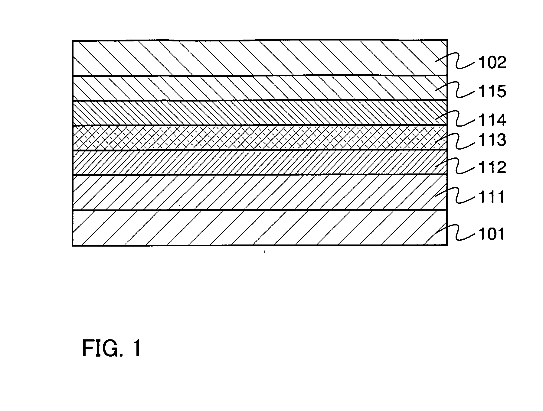
[0073] A mode of a light emitting element of the present invention is described with reference to FIG. 1.

[0074]FIG. 1 shows the light emitting element in which a first layer 111, a second layer 112, a third layer 113, a fourth layer 114, and a fifth layer 115 are interposed between a first electrode 101 and a second electrode 102.

[0075] This first layer is a layer formed to mix the carbazole derivative represented by General Formula (1) with the substance having an electron accepting property with respect to the carbazole derivative represented by General Formula (1). Since this first layer has a function of generating holes, the fist layer is hereinafter called a hole generating layer. The second layer 112 is a hole transporting layer, the third layer 113 is a light emitting layer, and the fourth layer 114 is an electron transporting layer. The fifth layer 115 is a layer having a function of generating electrons, hereinafter called an electron generating layer.

[0076] When voltag...

embodiment mode 2

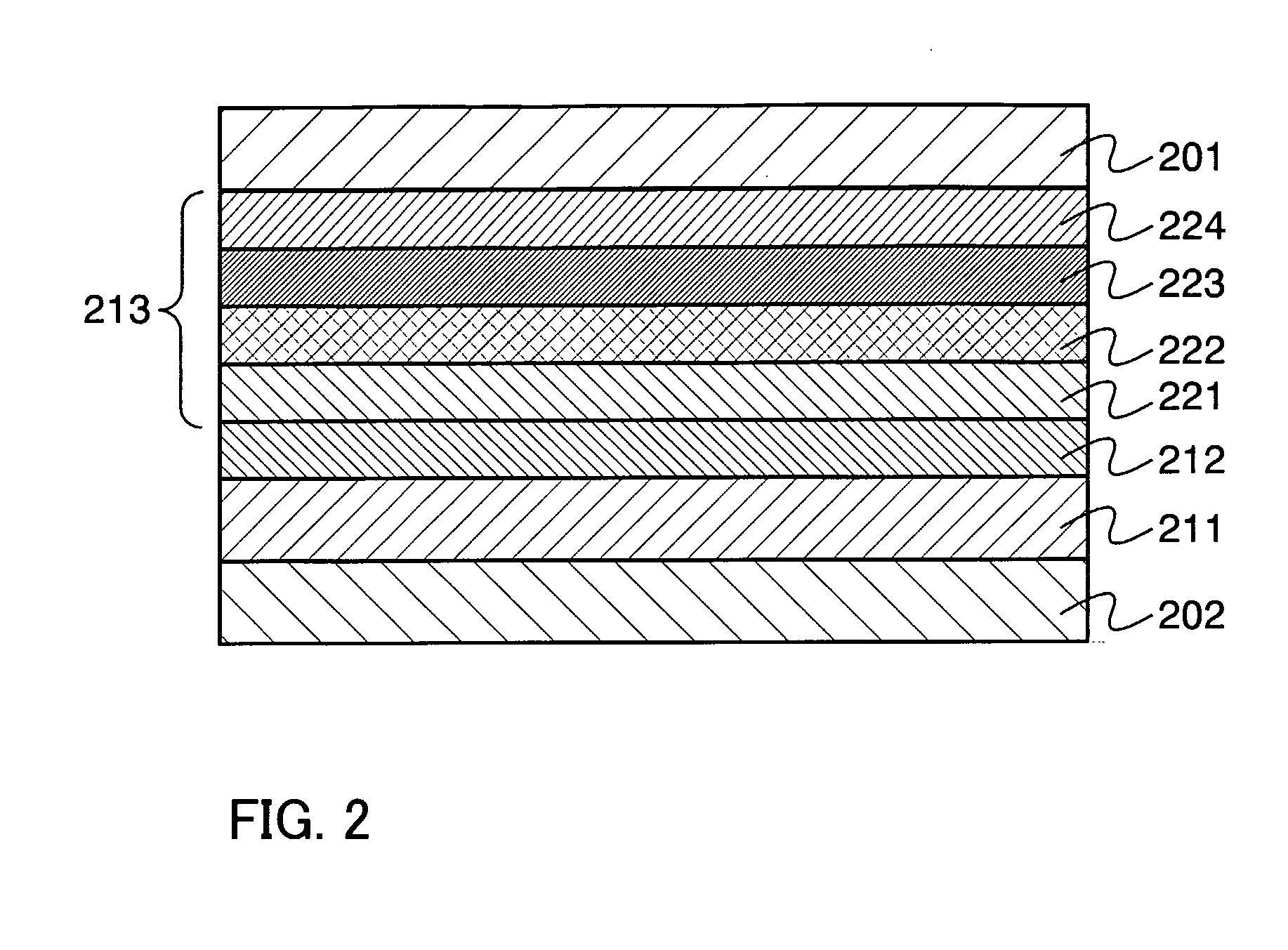
[0121] A mode of a light emitting element of the present invention is described with reference to FIG. 2.

[0122] In FIG. 2, a light emitting element in which a first layer 213, a second layer 212, and a third layer 211 are interposed between a first electrode 201 and a second electrode 202 is shown. The first layer 213 is formed by sequentially laminating an electron transporting layer 221, a light emitting layer 222, a hole transporting layer 223, and a hole generating layer 224. The second layer 212 generates electrons, and the third layer 211 generates holes.

[0123] Here, the hole generating layer 224 is provided closer to the first electrode 201 than the light emitting layer 222, and the electron transporting layer 221 is provided closer to the second electrode 202 than the light emitting layer 222. When voltage is applied to the first electrode 201 and the second electrode 202 so that potential of the first electrode 201 is higher than that of the second electrode 202, holes ar...

embodiment mode 3

[0141] In the light emitting element of the present invention, the number of malfunctions due to oxidation or crystallization of a compound can be decreased. By thickening a hole generating layer, a short circuit between electrodes can be prevented. In addition, by changing the thickness of the hole generating layer, light path length can be adjusted, light extraction efficiency can be increased, and light emission with good color purity can be obtained. Accordingly, by using the light emitting element of the present invention as a pixel, a favorable light emitting device, which has few display faults due to the malfunctions of the light emitting element, and which can provide image with favorable display color, can be obtained. In addition, by using the light emitting element of the present invention as a light source, a light emitting device which can favorably perform lighting with few faults due to the malfunctions of the light emitting element can be obtained.

[0142] The presen...


PUM

PropertyMeasurementUnit
thicknessaaaaaaaaaa
sizeaaaaaaaaaa
wavenumberaaaaaaaaaa

Abstract

An object of the present invention is to provide a light emitting element which has low driving voltage and can increase lifetime longer than a conventional light emitting element. One feature is to include a plurality of layers which includes a layer containing a light emitting substance between first and second electrodes, in which at least one layer of the plurality of layers contains a carbazole derivative represented by General Formula (1) and a substance having an electron accepting property with respect to the carbazole derivative represented by General Formula (1). By employing this structure, the above object can be achieved.

Description

TECHNICAL FIELD [0001] The present invention relates to a light emitting element having a structure in which a plurality of layers is interposed between a pair of electrodes, and especially relates to a structure of a layer which can be used as at least one layer of the plurality of layers. BACKGROUND ART [0002] A light emitting device utilizing light emission from an electroluminescent element (light emitting element) attracts attention as a device for displaying or lighting. [0003] As the light emitting element used in the light emitting device, a light emitting element having a structure in which a layer containing a luminescent compound is interposed between a pair of electrodes is well known. [0004] In such a light emitting element, one electrode functions as an anode, and the other electrode functions as a cathode. Holes injected from the anode side and electrons injected from the cathode side recombine to form excited state molecules, and when the molecules return to a ground...

Claims


Application Information

Patent Timeline
Patent Type & Authority Applications(United States)
IPC IPC(8): H01L51/54
CPCH01L51/0052H01L51/0059H01L51/006H01L51/0061H01L2251/5323H01L51/0081H01L51/5052H01L2251/305H01L2251/5315H01L51/0072Y10S428/917H10K85/636H10K85/633H10K85/631H10K85/615H10K85/324H10K85/6572H10K50/155H10K2102/101H10K2102/3031H10K2102/3026
Inventor NAKASHIMA, HARUENOMURA, RYOJIABE, HIROKOSEO, SATOSHISAKATA, JUNICHIROKUMAKI, DAISUKEIKEDA, HISAO
Owner SEMICON ENERGY LAB CO LTD
Why Eureka
Try Eureka