Method for fabricating a semiconductor device and apparatus for inspecting a semiconductor

Active Publication Date: 2007-07-26
SHARP KK
View PDF0 Cites 13 Cited by
  • Summary
  • Abstract
  • Description
  • Claims
  • Application Information

AI Technical Summary

Benefits of technology

[0038] With a method for manufacturing a semiconductor device and an apparatus for inspecting a semiconductor according to the present invention, it is possi

Problems solved by technology

Moreover, if laser processing is performed at a laser power far lower than the optimum laser power value, the amorphous silicon does not completely crystallize.
At a higher laser power, crystallization progresses, but a laser power even slightly higher than the optimum laser power value promotes re-crystallization of the amorphous silicon film, resulting in poor characteristics in the polycrystalline silicon film.
This hampers stable formation of the polycrystalline silicon film.
However, no monitoring methods have been conventionally described that permit the setting of the optimum laser p

Method used


Image

  • Method for fabricating a semiconductor device and apparatus for inspecting a semiconductor
  • Method for fabricating a semiconductor device and apparatus for inspecting a semiconductor
  • Method for fabricating a semiconductor device and apparatus for inspecting a semiconductor

Examples


Embodiment Construction

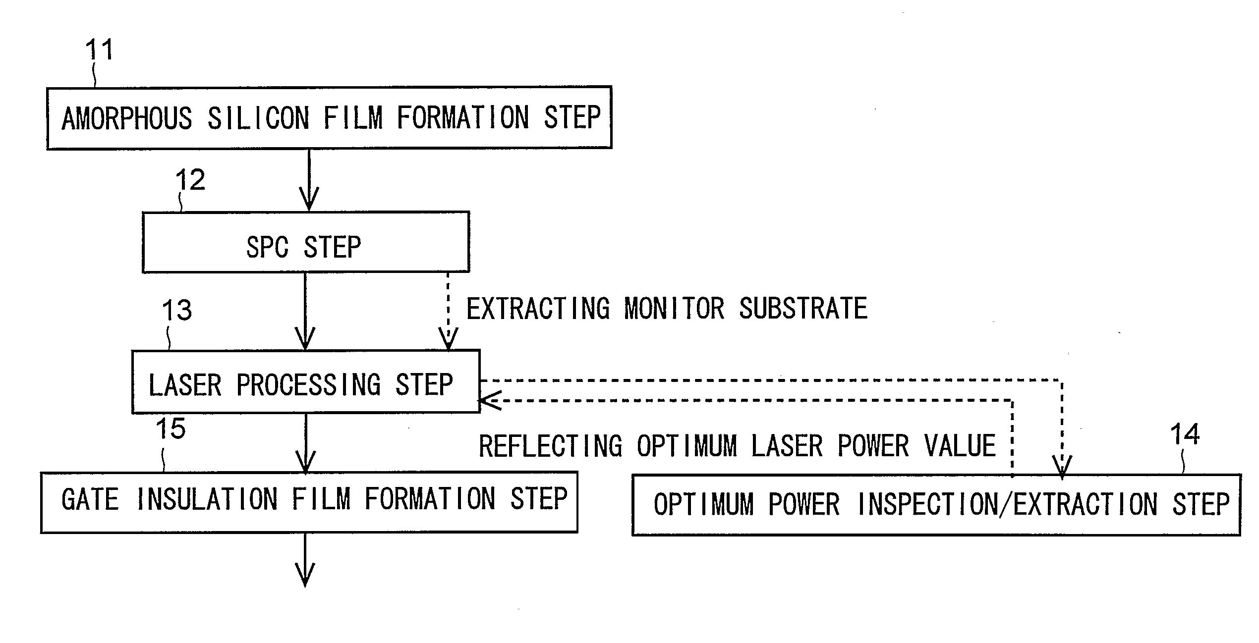
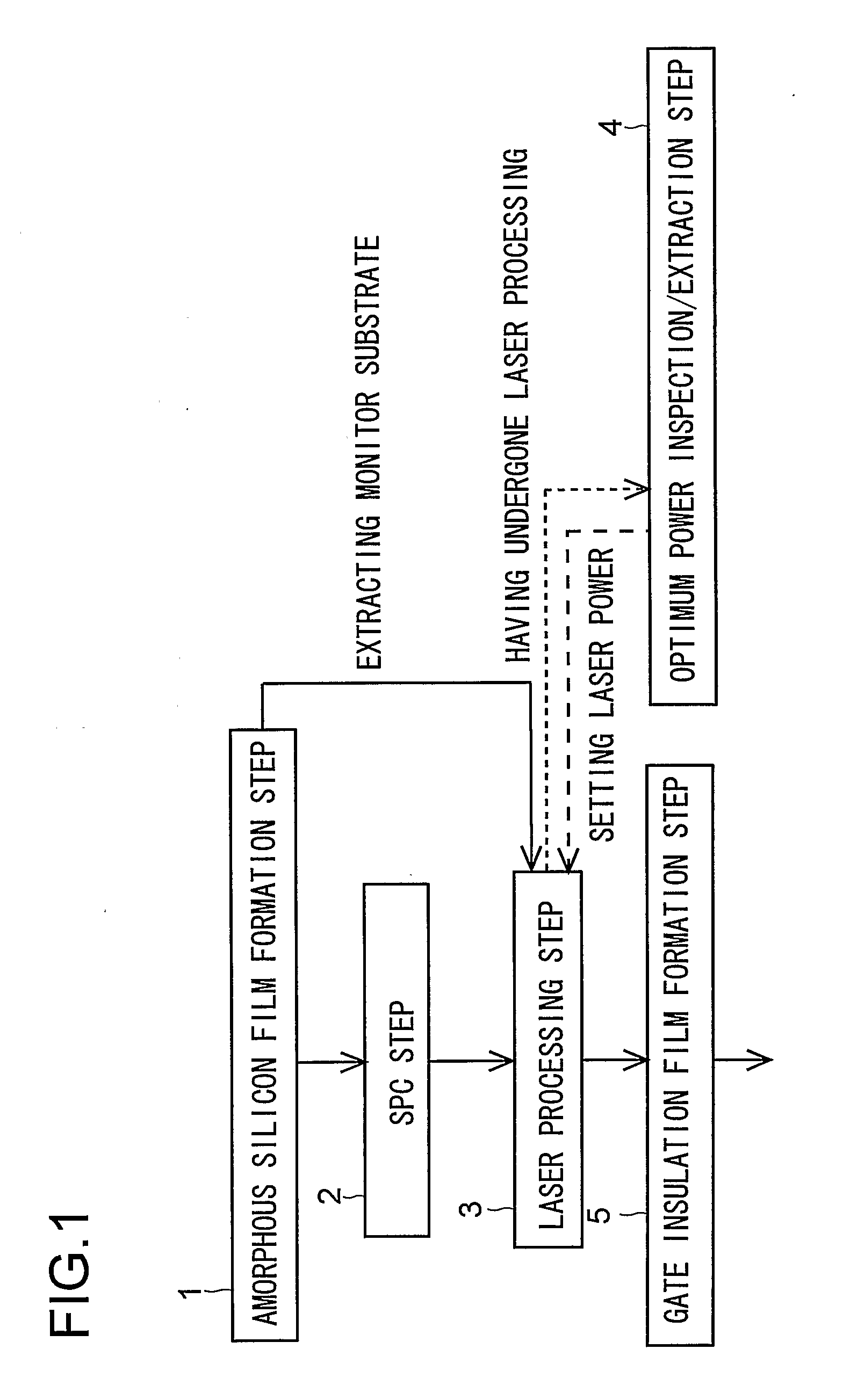
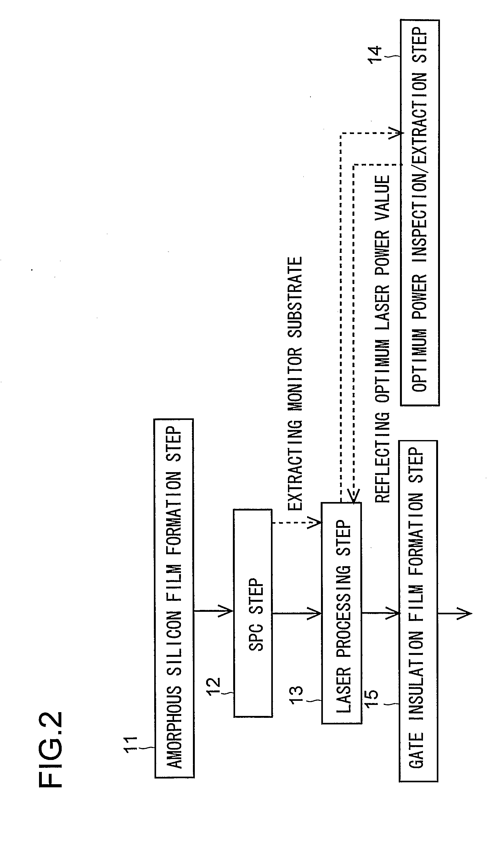
[0065] Hereinafter, a description will be given of examples of methods according to the present invention for producing polycrystalline silicon film by using a catalyst. FIG. 2 is a flow chart showing an example of a production method according to the invention. As shown in FIG. 2, in this embodiment, the method for producing polycrystalline silicon film by using a catalyst (the CGS, short for continuous grain silicon, method) includes: an amorphous silicon film formation step 11 for forming amorphous silicon film on a glass substrate by chemical vapor growth; an SPC step 12 for adding a crystallization-promoting metal element (for example, nickel) to the amorphous silicon film and then heating it so as to form crystalline silicon that extends starting from regions to which the metal element has been added; a laser processing step 13 for irradiating the amorphous silicon film having undergone the SPC step with laser so as to form polycrystalline silicon film over the entire area of ...


PUM

PropertyMeasurementUnit
Angleaaaaaaaaaa
Angleaaaaaaaaaa
Wavelengthaaaaaaaaaa

Abstract

In a method for fabricating a semiconductor device and an apparatus for inspecting a semiconductor, laser processing is performed at different laser powers at different positions on a monitor substrate from a plurality of substrates having undergone an SPC step, to form polycrystalline silicon film over the entire area of the substrate. Thereafter, in an optimum power inspection/extraction step, the polycrystalline silicon film formed with varying film quality on the monitor substrate is inspected on inspection equipment to determine the optimum laser power. Then, in a laser processing step, the surface of the subsequent substrates having undergone the SPC step is irradiated with laser at the optimum laser power. Thus, high-quality polycrystalline silicon film is formed over the entire area of the substrate.

Description

TECHNICAL FIELD [0001] The present invention relates to a method for fabricating a semiconductor device incorporating a circuit built with thin-film transistors (hereinafter TFTs), and also relates to an apparatus for inspecting a semiconductor. BACKGROUND ART [0002] TFTs using polycrystalline silicon film are being eagerly researched and developed for higher performance by different manufacturers with keen competition among them. In progress are various kinds of systematization of such TFTs with a view to realizing, for example, sheet computers and the like in the future. One way of obtaining higher performance with liquid crystal display devices is to increase the mobility of carriers in TFTs. For this purpose, polycrystalline silicon film is superseding amorphous silicon film for application in TFTs. Since, in TFTs using polycrystalline silicon film, the performance and quality of the polycrystalline silicon film is the key to enhanced TFT characteristics, it is becoming increasi...

Claims


Application Information

Patent Timeline
IPC IPC(8): H01L21/20H01L21/36H01L21/268H01L21/336H01L29/786
CPCB23K26/032H01L21/02422H01L21/02532H01L21/02672H01L21/02675H01L21/268H01L2924/0002H01L22/12H01L22/20H01L27/1285H01L2924/00
Inventor TAGUSA, YASUNOBU
Owner SHARP KK
Why Eureka
Try Eureka