Methods of making quantum dot films

a quantum dot and film technology, applied in the field of optical and electronic devices, can solve the problems of low yield, incompatibility of deposition with established silicon integrated circuit fabrication techniques, and unusually sensitive detectors

Active Publication Date: 2007-07-26
INVISAGE TECHNOLOGIES
View PDF7 Cites 89 Cited by
  • Summary
  • Abstract
  • Description
  • Claims
  • Application Information

AI Technical Summary

Benefits of technology

[0040] One or more embodiments include one or more of the following features. The film is substantially free of ligands attached to the outer surface of the fused nanocrystals. The outer surfaces of the fused nanocrystals include a material having a different composition than the core. The outer surfaces include at least one defect state. The at least one defect state includes at least one trap state for a hole during operation of the optical device. The outer surfaces include a semiconductor material. The outer surfaces include oxidized core material. The electrical network of fused nanocrystals provides a plurality of relatively low-resistance electrical paths from the first electrode to the second electrode. The film has an electrical resistance of at least about 25 k-Ohm/square. The electrical resistance of the film changes in response to irradiation by light. The electrical network of fused nanocrystals provides a plurality of electrical paths from the first electrode to the second electrode and at least some of those electrical paths undergo a change in electrical resistance in response to incident light. The film has a carrier mobility of between about 0.001 cm2/Vs and about 10 cm2/Vs. The film has a carrier

Problems solved by technology

These techniques can result in exceptionally sensitive detectors—normalized detectivity, D*, as high as 8×10¹⁰ Jones from PbS at room temperature for example—but their deposition is generally incompatible with established silicon integrated circuit fabrication techniques.
This non-monolithic process then necessitates a complex assembly procedure, resulting in low yie

Method used


Image

  • Methods of making quantum dot films
  • Methods of making quantum dot films
  • Methods of making quantum dot films

Examples


examples

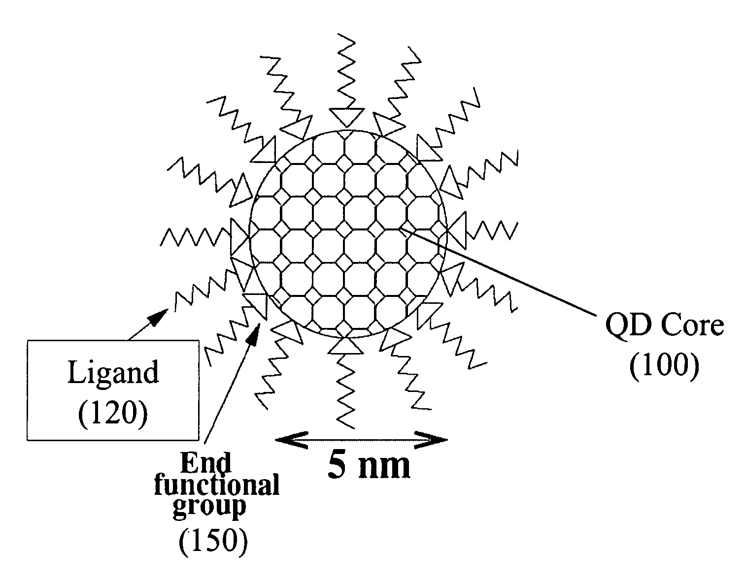
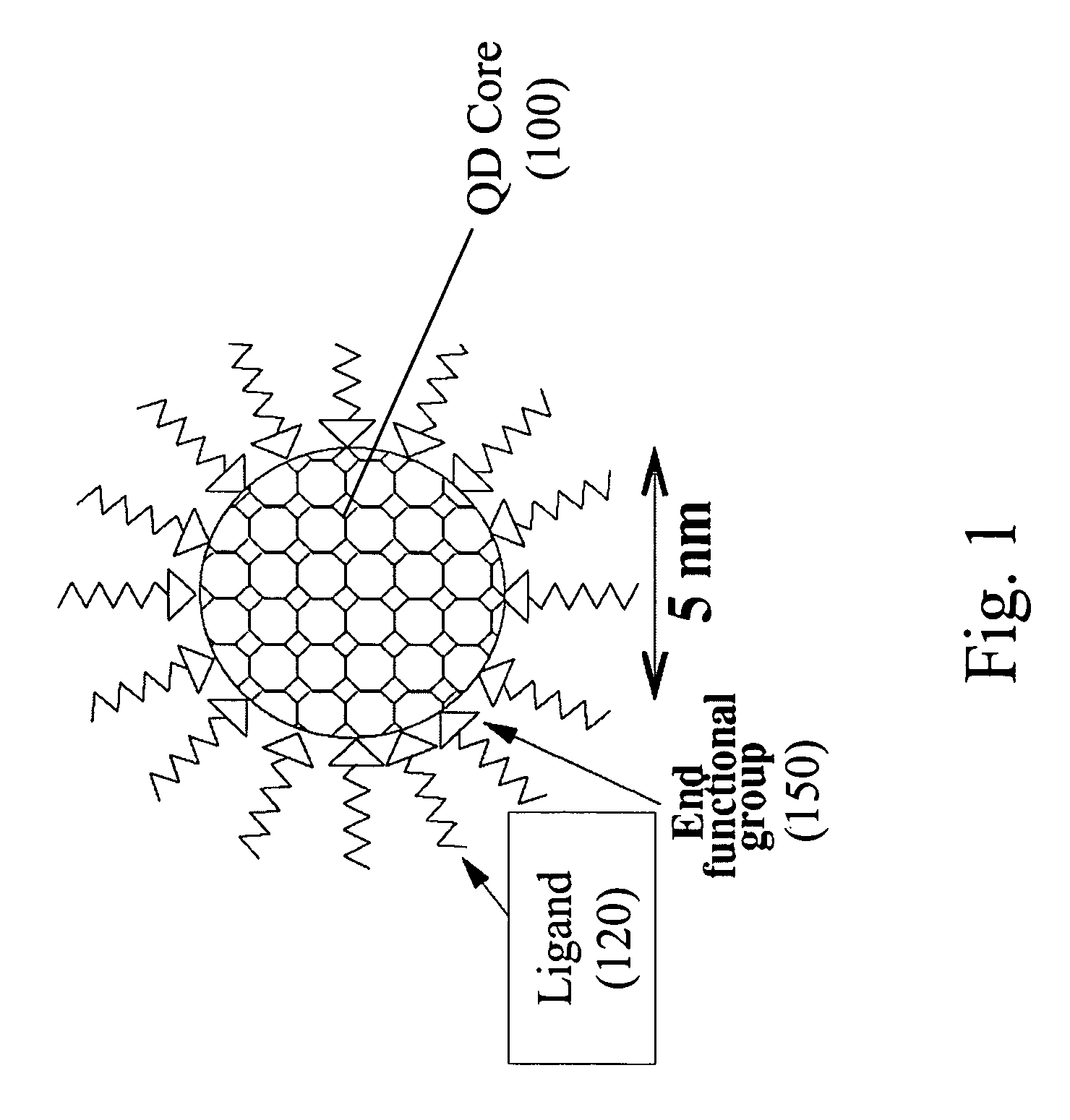
[0123] An exemplary photoconductive detector was made using a single layer of PbS QD nanocrystals spin-cast directly from a chloroform solution onto an interdigitated electrode array. The device structure is illustrated in FIG. 7A, and is analogous to the basic device of FIG. 4B. The parallel gold electrodes are supported by a glass substrate and have a height, width, and separation of 100 nm, 3 mm, 5 μm, respectively. The thickness of the QD layer was controlled through the concentration of the chloroform-QD solution and the spin-casting parameters. In studies carried out by the inventors the thickness ranged from 100 nm up to 500 nm.

[0124] The treatment of the surfaces of the QDs was an important determinant of photodetector performance. Devices made directly from QDs capped with oleic acid, as synthesized through an organometallic route, did not exhibit any measurable conductance, as the 2 nm-long oleate ligand inhibits carrier transport among QDs. A post-synthesis ligand exchan...


PUM

PropertyMeasurementUnit
Temperatureaaaaaaaaaa
Lengthaaaaaaaaaa

Abstract

Optical and optoelectronic devices and methods of making same. Under one aspect, an optical device includes an integrated circuit an array of conductive regions; and an optically sensitive material over at least a portion of the integrated circuit and in electrical communication with at least one conductive region of the array of conductive regions. Under another aspect, a method of forming a nanocrystalline film includes fabricating a plurality of nanocrystals having a plurality of first ligands attached to their outer surfaces; exchanging the first ligands for second ligands of different chemical composition than the first ligands; forming a film of the ligand-exchanged nanocrystals; removing the second ligands; and fusing the cores of adjacent nanocrystals in the film to form an electrical network of fused nanocrystals. Under another aspect, a film includes a network of fused nanocrystals, the nanocrystals having a core and an outer surface, wherein the core of at least a portion of the fused nanocrystals is in direct physical contact and electrical communication with the core of at least one adjacent fused nanocrystal, and wherein the film has substantially no defect states in the regions where the cores of the nanocrystals are fused.

Description

CROSS-REFERENCE TO RELATED APPLICATIONS [0001] This application claims the benefit under 35 U.S.C. §119(e) of U.S. Provisional Application Ser. No. 60 / 710,944, entitled “Method for Increasing Gain and Sensitivity from Spin-Cast Colloidal Quantum Dot Photodetectors,” filed Aug. 25, 2005, the entire contents of which are incorporated herein by reference. This application is also a continuation-in-part of U.S. application Ser. No. 11 / 325,655, filed Jan. 9, 2006, which claims priority from U.S. Provisional Application Ser. No. 60 / 641,766, filed Jan. 7, 2005, each of which are incorporated herein by reference. [0002] This application is also related to the following applications, the entire contents of which are incorporated herein by reference: [0003] U.S. Patent Application Serial No. (TBA), filed on even date herewith and entitled “Quantum Dot Optical Devices with Enhanced Gain and Sensitivity and Methods of Making Same;”[0004] U.S. Patent Application Serial No. (TBA), filed on even d...

Claims


Application Information

Patent Timeline
IPC IPC(8): G06F17/50
CPCB82Y10/00Y10S977/774C30B29/605H01L27/14601H01L27/305H01L29/22H01L31/0352H01L51/0038H01L51/0545H01L51/0566H01L51/4253H01L51/426C30B7/005H01L21/02422H01L21/02521H01L21/02601H01L21/02628Y02E10/549Y10S977/773Y10S438/962B82Y30/00G06F30/00H10K39/30H10K85/114H10K10/466H10K10/488H10K30/30H10K30/35
Inventor SARGENT, EDWARDKONSTANTATOS, GERASIMOSLEVINA, LARISSAHOWARD, IANKLEM, ETHAN J.D.CLIFFORD, JASON
Owner INVISAGE TECHNOLOGIES
Why Eureka
Try Eureka