
Polishing slurry for silicon oxide, additive liquid and polishing method

a technology of silicon oxide and polishing slurry, applied in the field of polishing slurry, can solve the problems of difficult control of polysilicon to a degree, and achieve the effect of high speed

Inactive Publication Date: 2007-08-02
HITACHI CHEM CO LTD
View PDF6 Cites 82 Cited by
  • Summary
  • Abstract
  • Description
  • Claims
  • Application Information

AI Technical Summary

Benefits of technology

[0054] The invention provides a polishing slurry and a polishing method which are capable of polishing a silicon oxide film on a polysilicon film at a high speed, and inhibiting the progress of polishing of a polysilicon film in exposed parts in a CMP technique in the manufacturing process of a semiconductor in which a silicon oxide film is polished.

Problems solved by technology

However, it has been difficult to control polysilicon to a degree where it can be used as a stopper, or to achieve a sufficiently large polishing rate ratio between a film to be polished and polysilicon either with a silica polishing slurry or a cerium oxide polishing slurry.

Method used


Image

  • Polishing slurry for silicon oxide, additive liquid and polishing method
  • Polishing slurry for silicon oxide, additive liquid and polishing method
  • Polishing slurry for silicon oxide, additive liquid and polishing method

Examples


example 1

[0161] The substrate below was subjected to CMP polishing under following conditions while a polishing slurry of the polishing slurry 1 was dropped on the pad attached to the platen, and evaluated as described below.

[0162]

[0163] Substrate 1: A blanket substrate of 8 inch diameter comprising a Si substrate having formed thereon a silicon oxide film (P—TEOS) of 0.8 μm thickness.

[0164] Substrate 2: A blanket substrate of 8 inch diameter comprising a Si substrate having formed thereon a silicon oxide film of 0.1 μm thickness and a polysilicon film of 0.4 μm thickness in this order.

[0165]

[0166] Polishing apparatus: MIRRA polishing machine, manufactured by AMAT, platen diameter 600 mm, rotary type

[0167] Polishing pad: IC-1000 / Suba 400 manufactured by Nitta Haas Incorporated, foamed double layer pad with a concentric groove

[0168] Polishing pressure: 25 kPa

[0169] Platen rotation number: 98 min−1

[0170] Polishing slurry flow rate: 200 ml / min

[0171] Polishing time: 1 min

[0172]

[0173] Si...

example 2

[0176] The polishing rates for a silicon oxide film and a polysilicon film were evaluated using a polishing slurry of the polishing slurry 2 under the same conditions as Example 1. The results of the evaluation indicate that the polishing rate for a silicon oxide film was 250 nm / min, the polishing rate for a polysilicon was 1.5 nm / min, and the ratio of the polishing rate for a silicon oxide film to the polishing rate for a polysilicon film was 167.

example 3

[0177] The polishing rates for a silicon oxide film and a polysilicon film were evaluated using a polishing slurry of the polishing slurry 3 under the same conditions as Example 1. The results of the evaluation indicate that the polishing rate for a silicon oxide film was 90 nm / min, the polishing rate for a polysilicon was 3.5 nm / min, and the ratio of the polishing rate for a silicon oxide film to the polishing rate for a polysilicon film was 26.


PUM

PropertyMeasurementUnit
Percent by massaaaaaaaaaa

Abstract

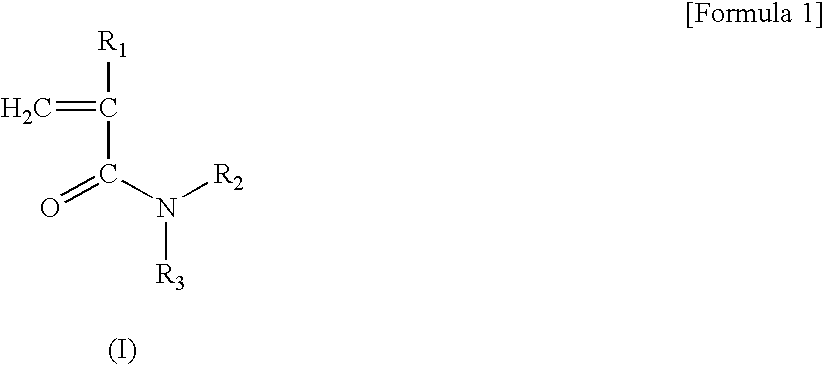
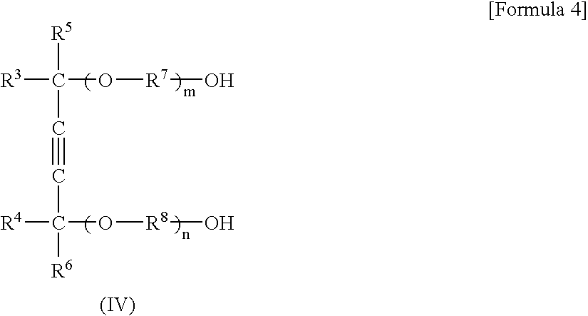
The polishing slurry of the invention is a polishing slurry for polishing a silicon oxide film on polysilicon, which contains an abrasive, polysilicon polishing inhibitor, and water. As the polishing inhibitor, it is preferable to use (1) a water-soluble polymer having a N-monosubstituted or N,N-disubstituted skeleton substituted by any member selected from the group consisting of acrylamide, methacrylamide, and α-substituted derivatives thereof, (2) polyethylene glycol, (3) an oxyethylene adduct of an acetylene-based diol, (4) a water-soluble organic compound having an acetylene bond, (5) an alkoxylated linear aliphatic alcohol, or (6) a copolymer containing polyvinyl pyrrolidone or vinyl pyrrolidone. There is provided a polishing method which is capable of polishing a silicon oxide film on a polysilicon film at a high speed, and inhibiting the progress of polishing of a polysilicon film in exposed parts in the manufacturing method for a semiconductor.

Description

BACKGROUND OF THE INVENTION [0001] 1. Field of the Invention [0002] The invention relates to a polishing slurry preferably used in the planarization process for dielectrics on substrate surfaces, which is a manufacturing technique for semiconductor devices, and particularly relates to a polishing slurry for silicon oxide on polysilicon, an additive liquid used in the polishing slurry, and a polishing method using the polishing slurry. [0003] 2. Description of the Related Art [0004] In the present ULSI semiconductor device manufacturing processes, processing techniques for achieving higher density and fineness have been developed. Among them, CMP (Chemical Mechanical Polishing) technique is becoming an essential technique in the manufacturing process for semiconductor devices, for planarization of interlayer dielectrics, shallow trench isolation, formation of plugs or buried metal wiring, and other purposes. [0005] In the manufacturing process for semiconductor devices, as chemical m...

Claims


Application Information

Patent Timeline
IPC IPC(8): B24D3/02B24B37/00C09K3/14H01L21/304
CPCC09G1/02H01L21/31053C09K3/1463C09K3/1409B24B1/00C09K3/14
Inventor NISHIYAMA, MASAYAENOMOTO, KAZUHIROFUKASAWA, MASATOAKUTSU, TOSHIAKIOTSUKI, YUUTOASHIZAWA, TORANOSUKE
Owner HITACHI CHEM CO LTD
Learn More