High-breakdown-voltage insulated gate semiconductor device

a technology of high-breakdown voltage and semiconductor devices, applied in the direction of semiconductor devices, basic electric elements, electrical equipment, etc., can solve problems such as anisotropy of electrical characteristics, and achieve excellent electrical characteristics and reduced electron mobility

Inactive Publication Date: 2007-08-02
PANASONIC CORP
View PDF8 Cites 16 Cited by
  • Summary
  • Abstract
  • Description
  • Claims
  • Application Information

AI Technical Summary

Benefits of technology

[0049] According to the semiconductor device of the present invention, when the electron mobility reduced due to step-bunching and other unfavorable interface states is improved, this can provide more excellent electrical characteristics than those of a known structure of a semiconductor device.

Problems solved by technology

The step bunches have a height of approximately 50 through 100 nm, leading to anisotropy in electrical characteristics.

Method used


Image

  • High-breakdown-voltage insulated gate semiconductor device
  • High-breakdown-voltage insulated gate semiconductor device
  • High-breakdown-voltage insulated gate semiconductor device

Examples


embodiment 1

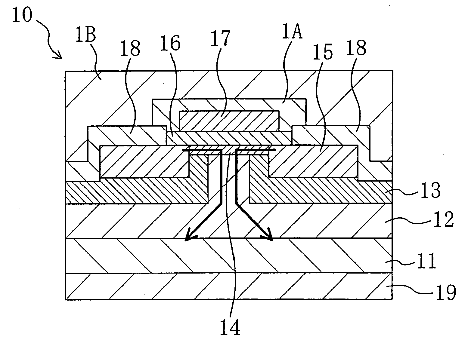
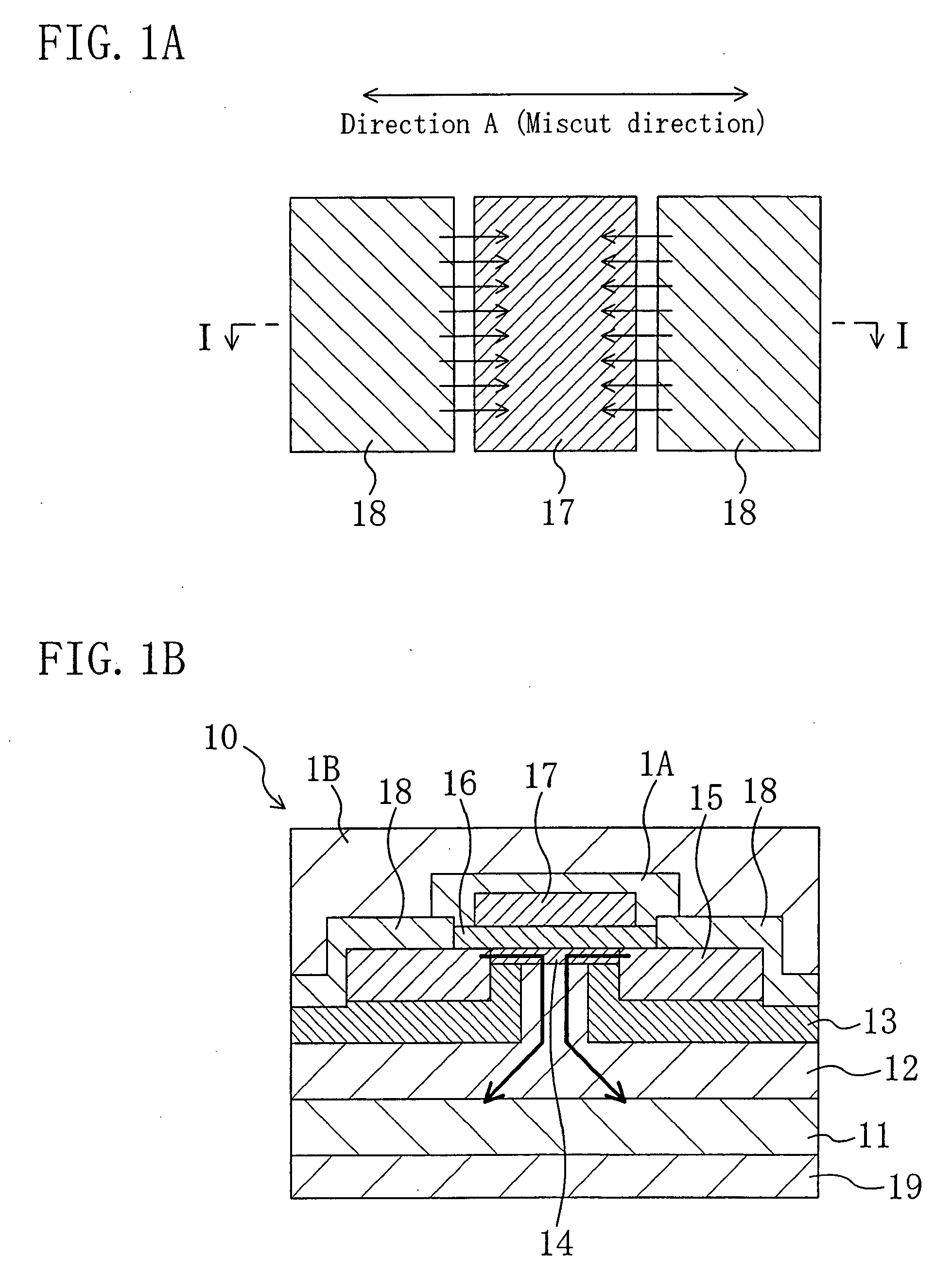
[0104] FIGS. 1(a) and 1(b) are cross-sectional views showing a joint between two unit cells of typical vertical accumulation-mode MOSFETs using a silicon carbide layer in a first embodiment. FIG. 1(a) is a plan view showing some of electrodes of the MOSFETs, and

[0105]FIG. 1(b) is a cross-sectional view taken along the line I-I in FIG. 1(a).

[0106] As shown in FIGS. 1(a) and 1(b), a semiconductor device of this embodiment has an n+-type 4H-SiC(0001) semiconductor substrate 11. The semiconductor substrate 11 has a surface miscut by approximately 8 degrees in the direction, and its resistivity is approximately 0.02 Ωcm2. An n-type 4H-SiC(0001) silicon carbide layer 12 is formed on the semiconductor substrate 11 to have a thickness of approximately 15 μm and doped with nitrogen at a concentration of 3×1015 cm−3. The n-type silicon carbide layer 12 is formed on the semiconductor substrate 11 by epitaxial growth, and the influence of the semiconductor substrate 11 causes the top surface...

embodiment 2

[0150] FIGS. 11(a) and 11(b) are cross-sectional views showing typical lateral accumulation-mode MOSFETs using a silicon carbide layer according to a second embodiment. FIG. 11(a) is a plan view showing some of electrodes of the MOSFETs when seen from above, and FIG. 11(b) is a cross-sectional view taken along the line VII-VII in FIG. 11(a).

[0151] As shown in FIGS. 11(a) and 11(b), a semiconductor device of this embodiment has a semi-insulating 4H-SiC(0001) semiconductor substrate 71. The semiconductor substrate 71 has a surface miscut by approximately 8 degrees in the direction. A 4H-SiC(0001) p-type silicon carbide layer 72 is formed on the semiconductor substrate 71 to have a thickness of approximately 5 μm and doped with aluminum at a concentration of 5×1015 cm−3.

[0152] An n-type channel layer 74 is formed in the middle region of the upper part of the p-type silicon carbide layer 72. In this embodiment, the channel layer 74 is a δ-doped layer obtained by alternately stacking ...


PUM


Abstract

In a semiconductor device of the present invention, the top surface of an n-type silicon carbide layer formed on a silicon carbide substrate is miscut from the (0001) plane in the <11-20> direction. A gate electrode, a source electrode and other elements are arranged such that in a channel region, the dominating current flows along a miscut direction. In the present invention, a gate insulating film is formed and then heat treatment is performed in an atmosphere containing a group-V element. In this way, the interface state density at the interface between the silicon carbide layer and the gate insulating film is reduced. As a result, the electron mobility becomes higher in a miscut direction A than in the direction perpendicular to the miscut direction A.

Description

TECHNICAL FIELD [0001] The present invention relates to a high-breakdown-voltage insulated gate semiconductor device using silicon carbide, and more particularly relates to a MOS field effect transistor (MOSFET) that provides a large-current switching device. BACKGROUND ART [0002] Silicon carbide (SiC) is a semiconductor with a higher hardness and a wider band gap than silicon (Si) and applied to power devices, environmentally resistant devices, high-temperature operating devices, high-frequency devices, and other devices. [0003] For example, MOSFETs as disclosed in Patent Document 1 that will be described below are known as representative switching devices using SiC. FIGS. 14(a) and 14(b) are diagrams showing typical vertical accumulation-mode MOSFETs using SiC. In a unit cell of a typical vertical MOSFET, a source electrode is arranged in the middle of the unit cell. On the other hand, FIGS. 14(a) and 14(b) show the arrangement of electrodes with a gate electrode arranged in the m...

Claims


Application Information

Patent Timeline
Patent Type & Authority Applications(United States)
IPC IPC(8): H01L29/76H01L21/04H01L29/04H01L29/06H01L29/24H01L29/36H01L29/423H01L29/78
CPCH01L21/049H01L29/045H01L29/0696H01L29/1608H01L29/365H01L29/7838H01L29/4238H01L29/518H01L29/66068H01L29/7802H01L29/41766
Inventor UCHIDA, MASAOKITABATAKE, MAKOTOKUSUMOTO, OSAMUYAMASHITA, KENYATAKAHASHI, KUNIMASAMIYANAGA, RYOKO
Owner PANASONIC CORP
Why Eureka
Try Eureka