

Semiconductor device and manufacturing method for the same
- Summary
- Abstract
- Description
- Claims
- Application Information
AI Technical Summary
Benefits of technology
Problems solved by technology
Method used
Image

Examples
first embodiment
(Manufacturing Method)
[0061]FIGS. 1 to 20 are cross sectional views showing a first aspect of a manufacturing method for a semiconductor device according to the first embodiment of the present invention. In the following, the manufacturing method according to Example 1 of the first embodiment is described with reference to these views.
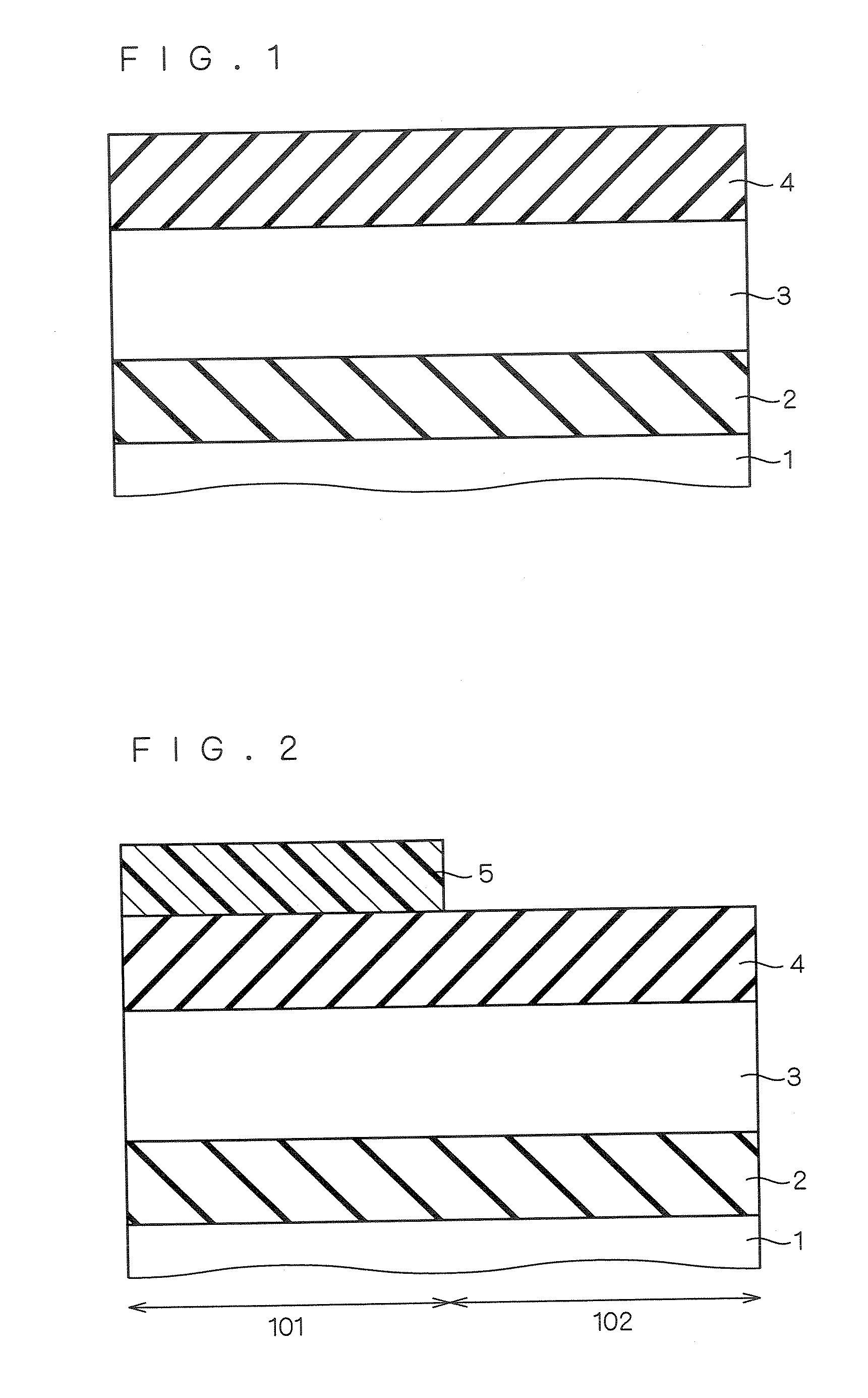
[0062]First, as shown in FIG. 1, a buried oxide film 2 having a film thickness of 10 nm to 1000 nm and a silicon layer 3 having a film thickness (first film thickness) of 30 nm to 200 nm are formed in sequence on a silicon support substrate 1, which is a semiconductor substrate, and thereby, an SOI substrate (structure) composed of the silicon support substrate 1, the buried oxide film 2 and the silicon layer 3 is obtained. Furthermore, a silicon nitride film 4 having a film thickness of 10 nm to 200 nm is formed on the silicon layer 3.
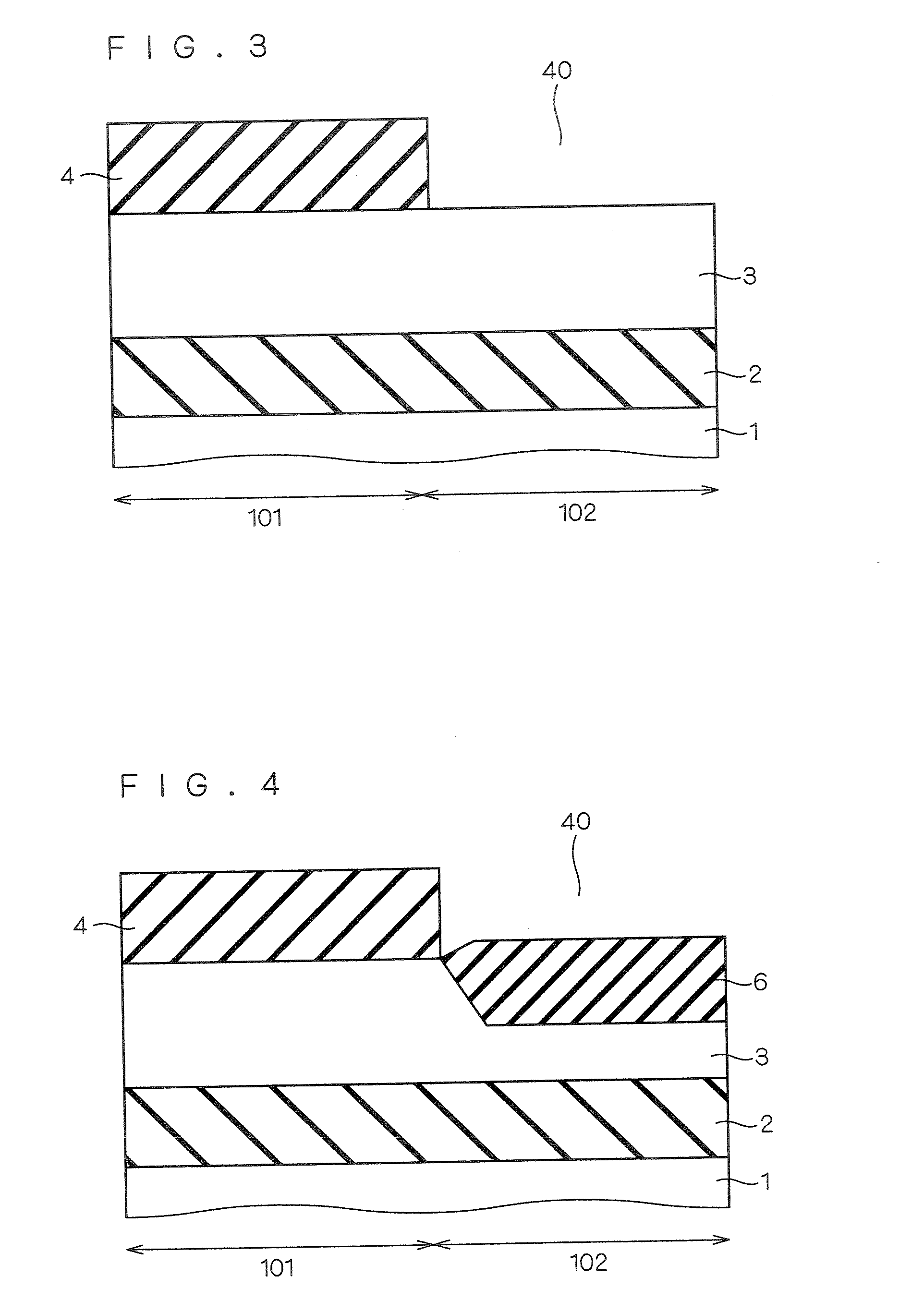
[0063]Next, as shown in FIG. 2, a resist film is applied on the entire surface and a resist pattern 5 for forming tren...
second embodiment
(Manufacturing Method)
[0144]FIGS. 64 to 67 are cross sectional views showing a portion of the first aspect of a manufacturing method for a semiconductor device according to the second embodiment of the present invention. In the following, the manufacturing method according to the second embodiment is described with reference to these figures.
[0145]As shown in FIG. 64, after the steps shown in FIGS. 1 to 16 in the first aspect of the first embodiment, the steps shown in FIGS. 21 to 40 in the second aspect and the steps shown in FIGS. 45 to 59 in the third aspect have been undertaken, in the same manner as in the first to third aspects of the first embodiment, gate electrodes 13 are formed, and silicon oxide film spacers 14 are formed on the sides of the gate electrodes 13.
[0146]Then, impurity ions 24 are injected into the silicon layer 3 using the gate electrodes 13 and the silicon oxide film spacers 14 as a mask so that low concentration regions 27 and 28 are formed in the thick fil...
third embodiment
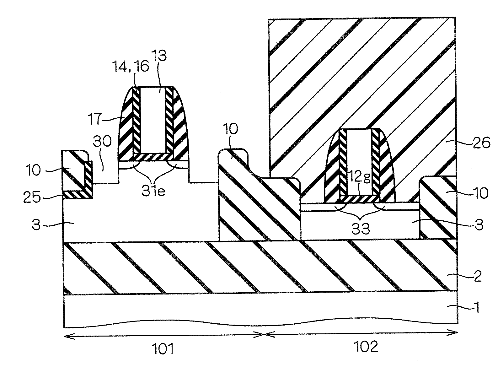
[0161]FIG. 68 is a cross sectional view showing the structure of a semiconductor device according to the third embodiment of the present invention. As shown in this figure, body thick film transistors Q1 and Q3 are formed on an SOI substrate composed of a silicon support substrate 1, a buried oxide film 2 and a silicon layer 3.
[0162]In the body thick film transistor Q1 (first transistor), recesses 30 are provided to source / drain regions 32 as shown in the first and second embodiments, and the source / drain regions 32 penetrate through the silicon layer 3 to reach the buried oxide film 2.
[0163]On the other hand, the source / drain regions 36 of the body thick film transistor Q3 (second transistor) are formed in upper layer parts of the silicon layer 3 without having recesses 30 and without penetrating through the silicon layer 3. Here, in the same manner as in the body thick film transistor Q1, extension / pocket regions 33e are formed in the surface of the silicon layer 3 beneath silicon...
PUM
 Abstract
Description
Claims
Application Information