
Receiver with colpitts differential oscillator, colpitts quadrature oscillator, and common-gate low noise amplifier

a receiver and differential oscillator technology, applied in the field of communication receivers, can solve the problems of preventing the widespread use of digital switching noise, and affecting the quality of signal transmission

Inactive Publication Date: 2007-08-02
UNIV OF WASHINGTON
View PDF2 Cites 12 Cited by
  • Summary
  • Abstract
  • Description
  • Claims
  • Application Information

AI Technical Summary

Problems solved by technology

Unfortunately, parasitic coupling in silicon technology, especially through the conductive silicon substrate, makes it possible for digital switching noise to corrupt the weak analog and RF signals.
In addition, LNA design involves tradeoffs between linearity, stability, input matching, and power consumption.
However, the higher noise figure and lower gain of the common-gate configuration impede it from being widely used.

Method used


Image

  • Receiver with colpitts differential oscillator, colpitts quadrature oscillator, and common-gate low noise amplifier
  • Receiver with colpitts differential oscillator, colpitts quadrature oscillator, and common-gate low noise amplifier
  • Receiver with colpitts differential oscillator, colpitts quadrature oscillator, and common-gate low noise amplifier

Examples


Embodiment Construction

[0028] In a conventional common-gate LNA, noise factor is given by F=1+ind2_·(11+gm⁢RS)2inS2_·(gm⁢RS1+gm⁢RS)2=1+ind2_inS2_⁢(1gm⁢RS)2(1)

With ind2=4kTγgd0Δf , inS2=4kTRS−1Δf and α=gm / gd0, (1) reduces to F=1+4⁢kT⁢ ⁢γ⁢ ⁢gd⁢ ⁢0⁢Δ⁢ ⁢f4⁢kTRS-1⁢Δ⁢ ⁢f⁢(1gm⁢RS)2=1+γ⁢ ⁢gd⁢ ⁢0gm2⁢RS=1+γα⁢❘gm⁢RS=1(2)

where α and γ are empirical process- and bias-dependent parameters, gm is the effective small signal transconductance, RS is the input impedance, F is the noise factor, gd0 is the drain-source conductance at zero drain-source voltage, k is Boltzmann's constant, T is the absolute temperature in Kelvins, inS is the noise current from source impedance, and ind is the channel noise of MOSFET. Embodiments of the present invention are based on the following observation, that is, in order to lower noise figure F, α in (2) should be effectively increased. This goal is met by increasing the effective small signal transconductance gm while keeping gd0 unchanged, as proposed in the current invention.

[0029]...


PUM


Abstract

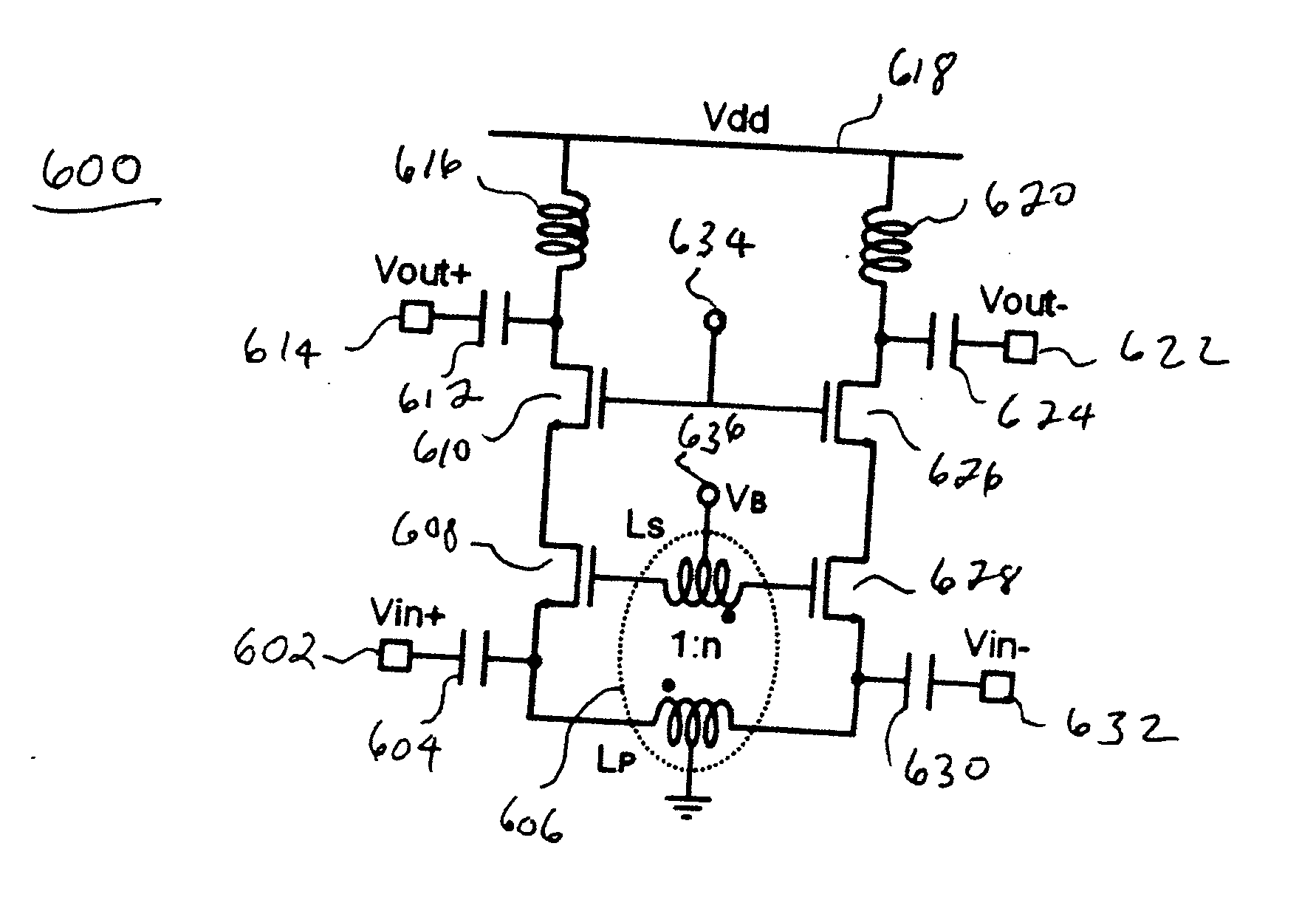
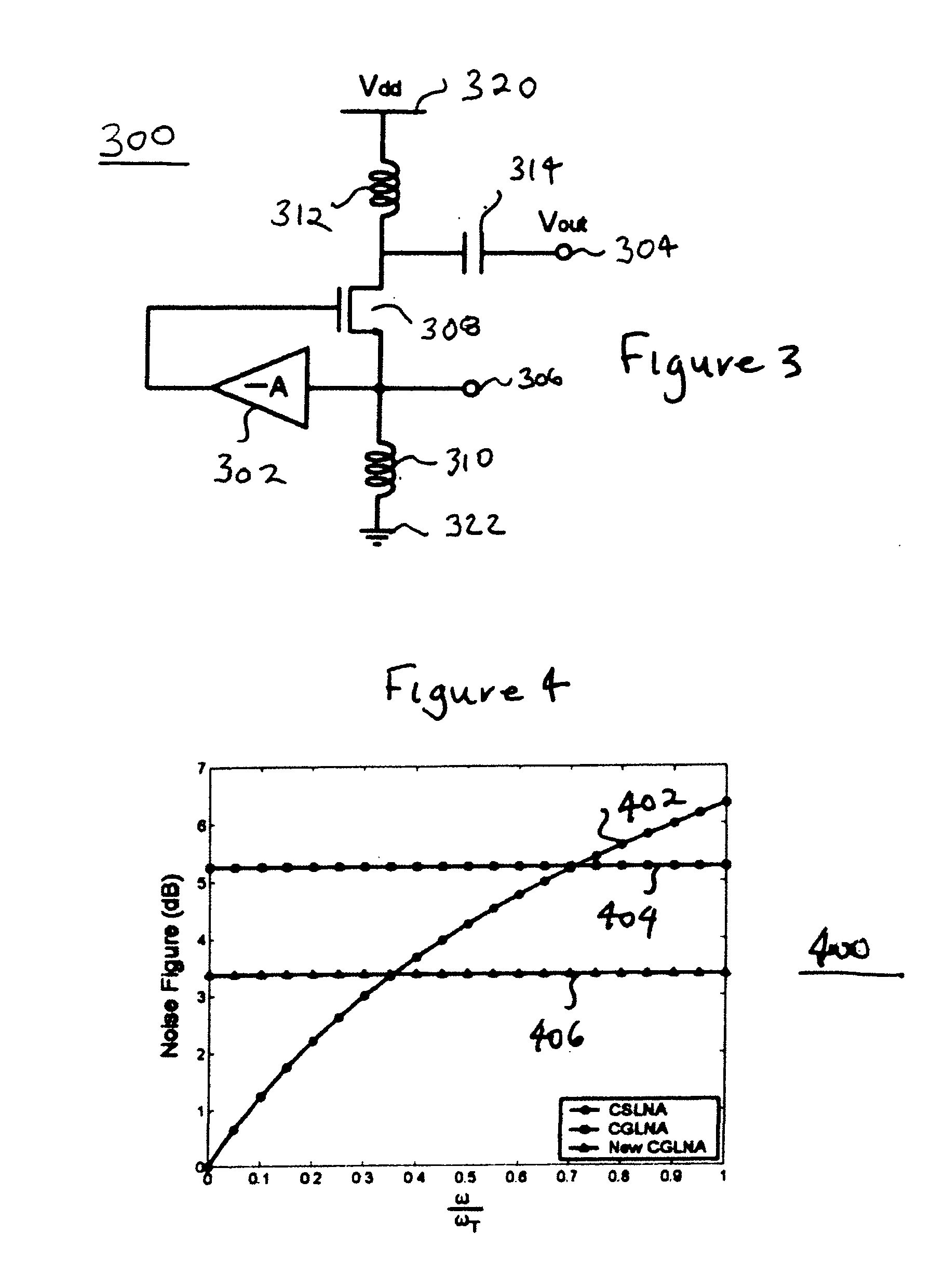
Embodiments of the present invention include a common-gate amplifier having an input terminal and an output terminal, a transistor having a source, a drain, and a gate, four inductors, and two capacitors, and a negative amplification circuitry. The negative amplification circuitry has an input terminal to receive an RF signal. The negative amplification circuitry applies negative or zero amplification to the RF signal and outputs the negative or zero amplified signal on an output terminal. Alternative embodiments include a Colpitts differential oscillator, which includes two Colpitts single-ended oscillators. Each Colpitts single-ended oscillator includes a transistor. The source of the transistor in one Colpitts single-ended oscillator may be capacitively coupled to the gate of the transistor in the other Colpitts single-ended oscillator.

Description

BACKGROUND [0001] 1. Field [0002] Embodiments of the present invention are related to communication receivers and, in particular, to receivers that include voltage-controlled oscillators (VCO) and low-noise amplifiers (LNA). [0003] 2. Discussion of Related Art [0004] Wireless communication systems commonly include cellular phones, radios, and radar systems, for example. A typical wireless system includes a receiver that receives a signal carried on an electromagnetic wave, such as a radio frequency (RF) signal. [0005] The ever-increasing interest in wireless communication systems also is emphasizing higher levels of integration, more complex functionalities and lower cost in integrated circuit (IC) implementations. Recently, complementary metal oxide semiconductor (CMOS) has emerged as viable alternative for RF and microwave integrated circuit (MIC) designs owing to the continued scaling of minimum feature size. The ability to integrate complex digital signal processing functions ma...

Claims


Application Information

Patent Timeline
IPC IPC(8): H03B5/08
CPCH03B27/00H03B2200/0008H03B5/1243H03B5/1296H03B5/1215H03B5/1228
Inventor LI, XIAOYONGALLSTOT, DAVID J.
Owner UNIV OF WASHINGTON
Learn More