Solid-state image pickup device

Active Publication Date: 2007-08-02
SONY SEMICON SOLUTIONS CORP
View PDF6 Cites 38 Cited by
  • Summary
  • Abstract
  • Description
  • Claims
  • Application Information

AI Technical Summary

Benefits of technology

[0015] In a solid-state image pickup device according to an embodiment of the present invention, for each of the pixels, lines extending in the vertical and horizontal directions are disposed on pixels diagonally arrayed so as to lie diagonally along sides of a photoelectric conversion unit when reaching around the photoelectric conversion unit. With this arrangement, obstruction of light collection of the photoelectric conv

Problems solved by technology

However, when miniaturization of pixels is promoted, or when a pixel transistor is shared by a plurality of photodiodes, light incident on each photodiode may be obstructed, particularly in a CMOS image sensor having

Method used


Image

  • Solid-state image pickup device
  • Solid-state image pickup device
  • Solid-state image pickup device

Examples


first embodiment

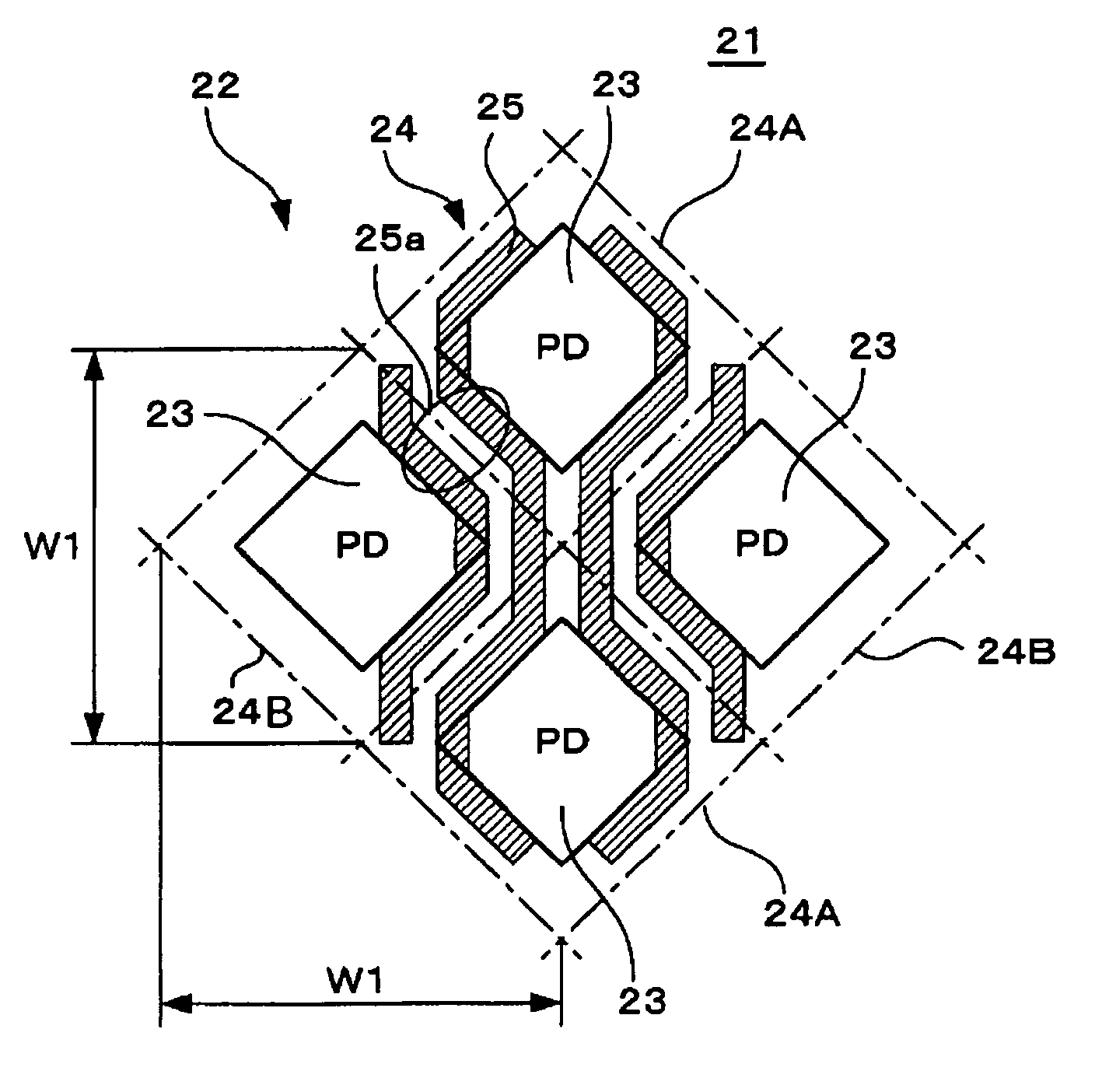
[0041]FIG. 1 illustrates a solid-state image pickup device according to an embodiment of the present invention, that is, a CMOS image sensor according to a The figure schematically illustrates a wiring layout in an image pickup area using an example of lines arranged in the vertical direction. A CMOS image sensor 21 according to the present embodiment includes a plurality of pixels 24 each having a photodiode (PD) 23 serving as a photoelectric conversion unit and a plurality of MOS transistors (not shown). The pixels 24 are diagonally and two-dimensionally arranged forming a so-called diagonal pixel array. Specifically, the CMOS image sensor 21 includes a first pixel group 23A, which includes a plurality of pixels 24A two-dimensionally arranged in a grid-like pattern at a predetermined pitch W1 in the vertical and horizontal directions, and a second pixel group, which includes a plurality of pixels 24B two-dimensionally arranged in a similar grid-like pattern. Each of the pixels 24...

second embodiment

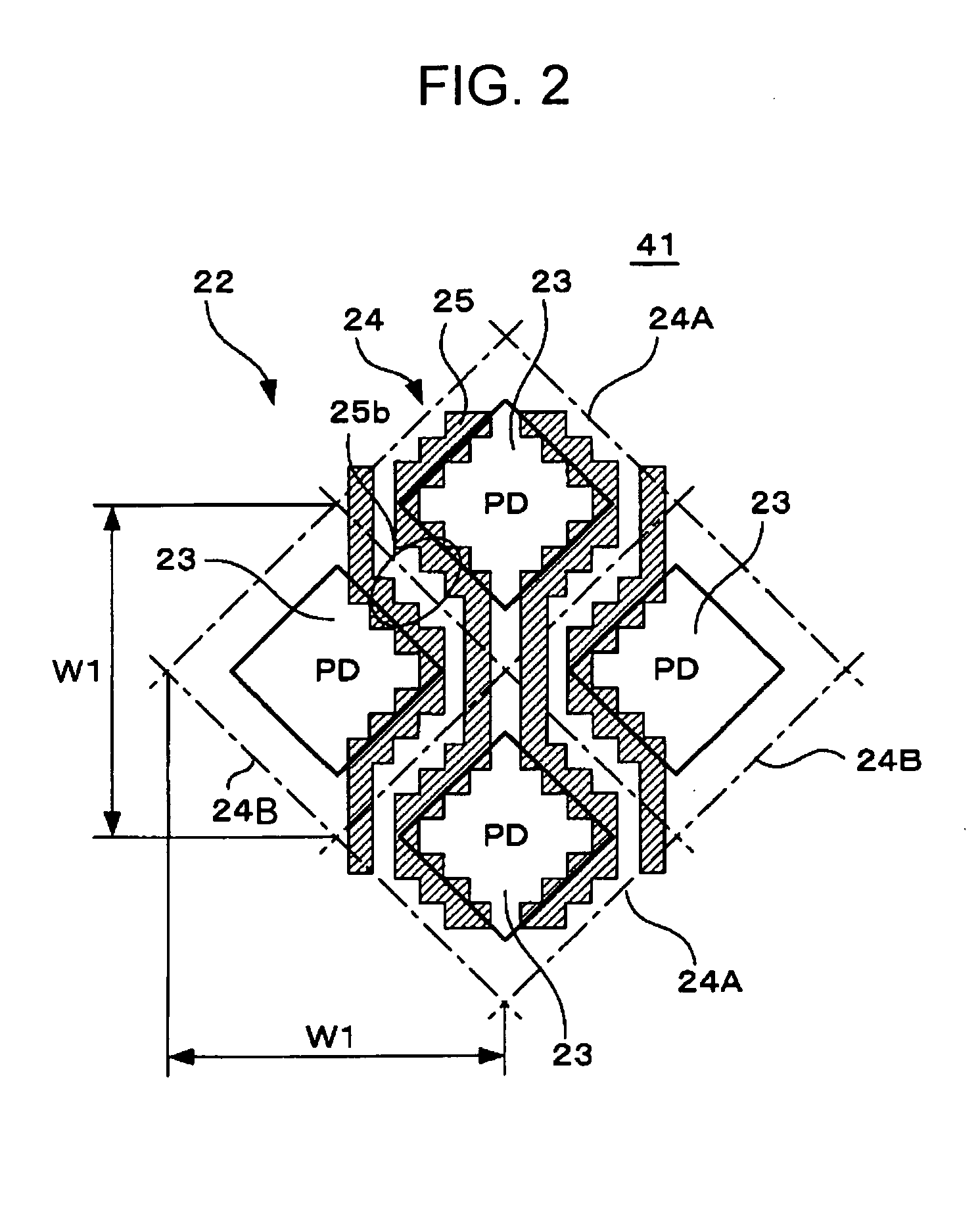
[0053]FIG. 2 illustrates a solid-state image pickup device according to an embodiment of the present invention, that is, a CMOS image sensor 41 according to a The figure schematically illustrates a wiring layout in an image pickup area using an example of lines arranged in the vertical direction. Similarly to the CMOS sensor 21 described above, the CMOS image sensor 41 according to the present embodiment includes a plurality of pixels 24 each having a photodiode (PD) 23 serving as a photoelectric conversion unit and a plurality of MOS transistors (not shown). The pixels 24 are two-dimensionally and diagonally arranged forming a so-called diagonal pixel array. Specifically, the CMOS image sensor 41 includes a first pixel group 23A, which includes a plurality of pixels 24A two-dimensionally arranged in a grid-like pattern at a predetermined pitch W1 in vertical and horizontal directions, and a second pixel group, which includes a plurality of pixels 24B two-dimensionally arranged in ...

third embodiment

[0064] the present invention can be applied to a CMOS image sensor in which a predetermined pixel transistor is shared by photodiodes corresponding to a plurality of pixels (for example, two pixels, three pixels, four pixels). FIG. 12 illustrates an equivalent circuit of a CMOS image sensor in which a reset transistor Tr2, an amplifying transistor Tr3, and a selection transistor Tr4 are shared by two pixels.

[0065] In this CMOS image sensor, photodiodes 2a and 2b for two pixels are connected to the sources of transfer transistors Tr1a and Tr1b, respectively. For each pair of pixels, the gates of the transfer transistors Tr1a and Tr1b are connected to the transfer lines 11A and 11B, respectively. The drains of the transfer transistors Tr1a and Tr1b are commonly connected to the reset transistor Tr2, and a so-called floating diffusion (FD) provided between the drains of the transfer transistors Tr1a and Tr1b and the source of the reset transistor Tr2 is connected to the gate of the amp...


PUM


Abstract

A solid-state image pickup device includes pixels diagonally arranged, each including a photoelectric conversion unit and a plurality of transistors and wiring extending in the vertical and horizontal directions which is diagonally arranged around the photoelectric conversion unit in each of the pixels so that at least one portion of the wiring is arranged along at least one side of the photoelectric conversion unit.

Description

CROSS REFERENCES TO RELATED APPLICATIONS [0001] The present invention contains subject matter related to Japanese Patent Application JP 2006-019367 filed in the Japanese Patent Office on Jan. 27, 2006, the entire contents of which are incorporated herein by reference. BACKGROUND OF THE INVENTION [0002] 1. Field of the Invention The present invention relates to solid-state image pickup devices. In particular, the present invention relates to a solid-state image pickup device such as a CMOS (complementary metal oxide semiconductor) image sensor having pixels each including a conversion unit converting charge generated by a photoelectric conversion unit into pixel signals. Such a CMOS image sensor is produced by applying or appropriately employing a CMOS process. [0003] The solid-state image pickup device can be an element type formed as one chip or be composed of a plurality of chips. [0004] 2. Description of the Related Art [0005] CMOS image sensors have a plurality of pixels arrange...

Claims


Application Information

Patent Timeline
IPC IPC(8): H04N5/335H01L27/146H04N5/349H04N5/369H04N5/374
CPCH01L27/14603H04N5/335H01L27/1462H01L27/14609H04N25/00
Inventor MARUYAMA, SHUNSUKEFUJIMAGARI, JUNICHIROWAKANO, TOSHIFUMITORII, MOTONOBUHOSHI, HIRONORIKIKUCHI, KOJI
Owner SONY SEMICON SOLUTIONS CORP
Why Eureka
Try Eureka