Charged particle optical apparatus with aberration corrector

a technology of aberration correction and optical apparatus, which is applied in the field of scanning electron microscope, can solve the problems of not being able to manufacture sem and backscattered electron microscopes within the reasonable price, and the field in such a degree as to remove aberration of charged particle beams having such high energy is very expensive, so as to achieve the effect of reducing the number of power supplies, minimizing beam spots, and improving operation performan

Active Publication Date: 2007-08-09
HITACHI HIGH-TECH CORP
View PDF6 Cites 26 Cited by
  • Summary
  • Abstract
  • Description
  • Claims
  • Application Information

AI Technical Summary

Benefits of technology

[0018]Thereby, in the case of electromagnetic lens, the power supply connected can be reduced in principle, only to one current source, while in the case of the complex type multipole lens, such power supply connected can be reduced to a couple of current source and voltage source in the multipole lens in each stage. The number of power supplies can effectively reduced by supplying the current source and voltage source from a complex power supply provided with both the current source and voltage source.

Problems solved by technology

In current, a power supply which is capable of supplying, with the required stability, an electromagnetic field in such a degree as removing aberration of the charged particle beam having such higher energy is very expensive.
Accordingly, in the case where the drive power supplies are provided in accordance with the number of poles, it is no longer possible to manufacture the SEM and b

Method used


Image

  • Charged particle optical apparatus with aberration corrector
  • Charged particle optical apparatus with aberration corrector
  • Charged particle optical apparatus with aberration corrector

Examples


first embodiment

[0032]A first embodiment of the present invention will be explained with reference to the accompanying drawings.

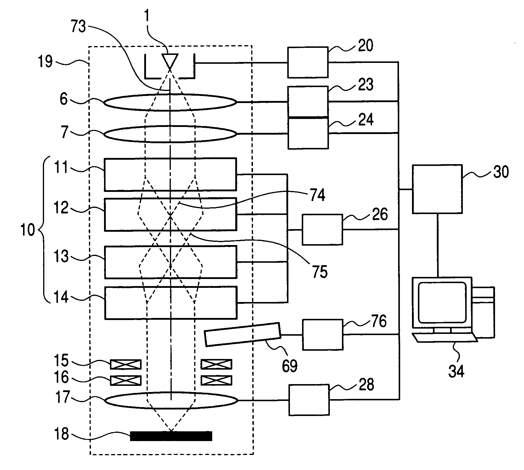
[0033]FIG. 1 shows an embodiment of a scanning electron microscope (SEM) which is capable of correcting chromatic aberration. In FIG. 1, the principal elements of an electronic optical system of SEM are indicated. The electron beam emitted from an electron source 1 focuses cross-over at the adequate location for an objective lens 17 after adjustment in amount of beam current with a converging lenses 6 and 7. This electron beam is further projected with demagnification projection to the surface of a specimen 8 using the objective lens 17 to attain beam probe. Amount of secondary electron generated by irradiation of electron is allocated for each location at the surface of specimen by scanning the beam probe at the specimen surface with deflection coils 15, 16 to obtain so-called “scanning electron microscope image (SEM image)” through visualization. The elements which are n...

second embodiment

[0045]In the first embodiment, the scanning electron microscope which can correct chromatic aberration has been explained but the charged particle beam generated by an electronic optical system includes spherical aberration in addition to chromatic aberration and such spherical aberration must also be eliminated in order to further converge the beam spot.

[0046]Moreover, a kind of aberration occupying a greater part in the charged particle beam is different depending on an accelerating voltage. In the SEM and backscattered electron microscope, the accelerating voltage used actually is ranged from about 1 kV to about 100 kV and the range from several hundreds volts to about 10 kV of the accelerating voltage is called the low acceleration region and the range from 10 kV to 100 kV thereof is called the high acceleration region. Here, in the low acceleration region, the charged particle beam includes both chromatic aberration and spherical aberration almost in the equal rate. On the othe...

third embodiment

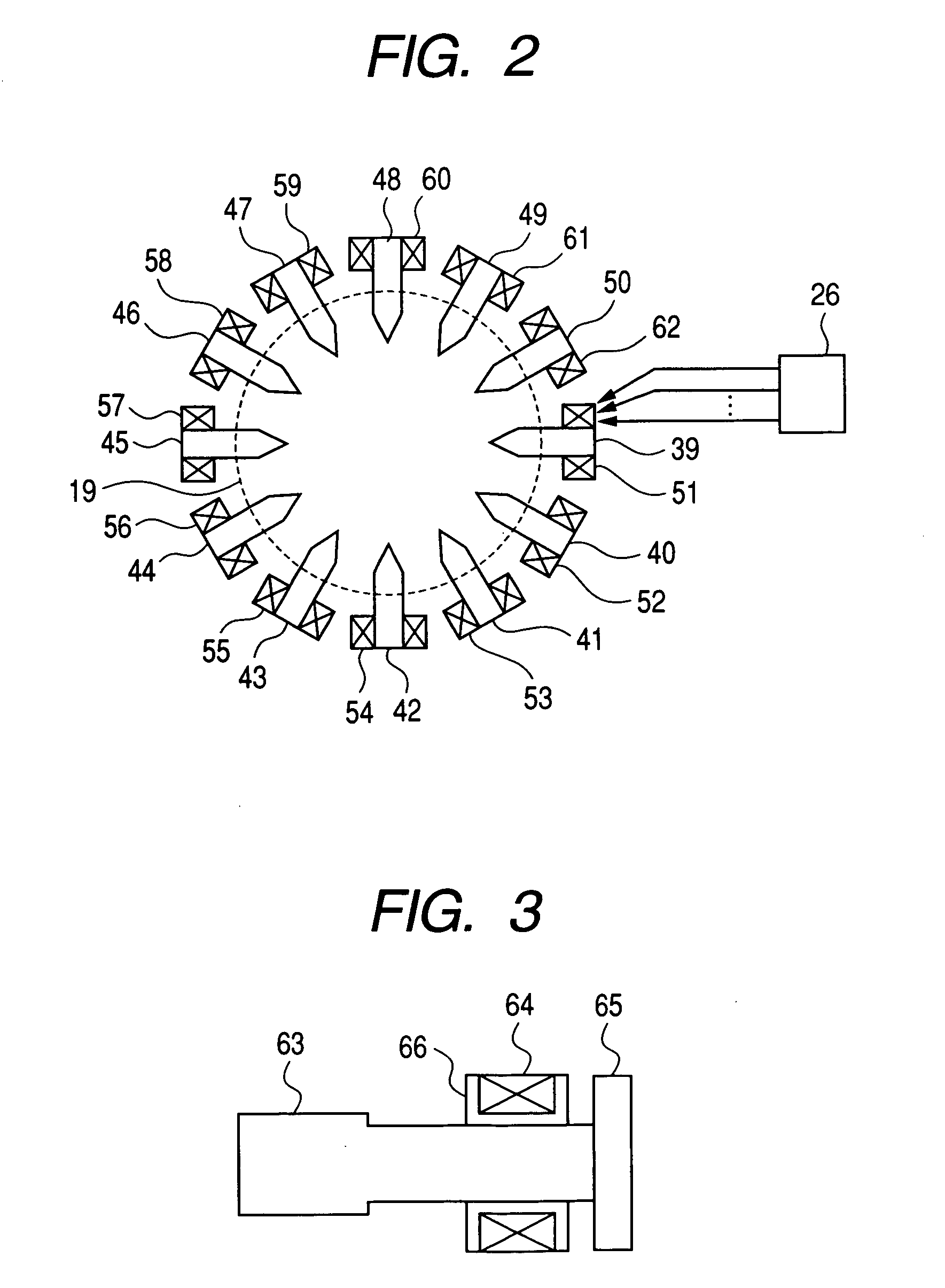
[0075]FIG. 11 shows an example of structure of a defective review SEM (DR-SEM) mounting the aberration corrector. FIG. 11 shows the structure attained by adding a detector 69b to the structure of FIG. 10. The detector 69b is arranged to the position different from the position symmetrical to the detector 69. Since the amount of secondary electrons detected from the detectors 69 and 69b depending on the structure of the specimen are different, the structure of specimen can be assumed and detected, on the contrary, by comparing the data obtained from both detectors. Data comparing operation can be executed with the computer 102.


PUM


Abstract

When an accelerating voltage and operating distance are changed, an excitation current and a pole voltage of an aberration corrector must also be changed. Moreover, different multipole voltages or currents must be added individually for each pole in order to superpose multipoles. In view of overcoming the problems explained above, the charged particle optical apparatus of the present invention comprises an excitation device including, to give excitation to form a multipole field to each pole of the multipole lens, electromagnetic type quadrupole of four stages arranged along an optical axis of charged particle beam, electromagnetic type quadrupole of two stages for superposing distribution of voltage similar to distribution of magnetic potential of the electromagnetic type quadrupole of two stages at the center of the electromagnetic type quadrupole of four stages, and electromagnetic type octupole for superposing magnetic potential at least to three multipoles among that of four stages and also comprises a first power supply group for driving the same excitation device and a second power supply group for impressing voltages.

Description

CLAIM OF PRIORITY[0001]The present application claims priority from Japanese application JP 2006-026500 filed on Feb. 3, 2006, the content of which is hereby incorporated by reference into this application.FIELD OF THE INVENTION[0002]The present invention relates to a technology to minimize beam spot of an electron beam apparatus and more specifically to a scanning electron microscope (SEM), a critical dimension SEM (CD-SEM), and an electron beam drawing apparatus or the like.BACKGROUND OF THE INVENTION[0003]In an apparatus such as a critical dimension SEM for measuring pattern size of semiconductor device with higher accuracy, experience in use of ultra-fine device pattern in recent years requires attaining of resolution of about 3 to 1 mm using the electron beam in accelerating voltage of 1 kV or lower in view of protecting a specimen. In order to satisfy the requirement explained above, a diameter of electron beam (spot size) on the surface of specimen must be reduced to a size o...

Claims


Application Information

Patent Timeline
IPC IPC(8): G21K7/00
CPCH01J37/153H01J2237/1534H01J37/28
Inventor NAKANO, TOMONORIYOSHIDA, TAKAHO
Owner HITACHI HIGH-TECH CORP
Why Eureka
Try Eureka