Finfet-based SRAM with feedback

a sram and feedback technology, applied in the field of memory devices, can solve the problems of increasing transistor leakage and parameter variation, compromising cell stability, etc., and achieve the effects of reducing leakage current, reducing the area of memory cells, and sufficient noise margins

Inactive Publication Date: 2007-08-09
RGT UNIV OF CALIFORNIA
View PDF8 Cites 52 Cited by
  • Summary
  • Abstract
  • Description
  • Claims
  • Application Information

AI Technical Summary

Benefits of technology

[0011] According to one or more aspects of the invention, memory cell architectures are described which provide data retention in a stable manner with sufficient noise margins during standby, read access, and write access. Furthermore, the invention can provide reductions in leakage current and even reduce the area of the memory cell.

Problems solved by technology

Notably, however, increased transistor leakage and parameter variation present challenges for scaling of conventional six-transistor (6-T) SRAM cells.
In order to limit static power dissipation in large caches, lower supply voltage can be used; however, a low supply voltage coupled with large transistor variability compromises cell stability, measured as the static noise margin.

Method used


Image

  • Finfet-based SRAM with feedback
  • Finfet-based SRAM with feedback
  • Finfet-based SRAM with feedback

Examples


example 1

FinFET Design and Modeling

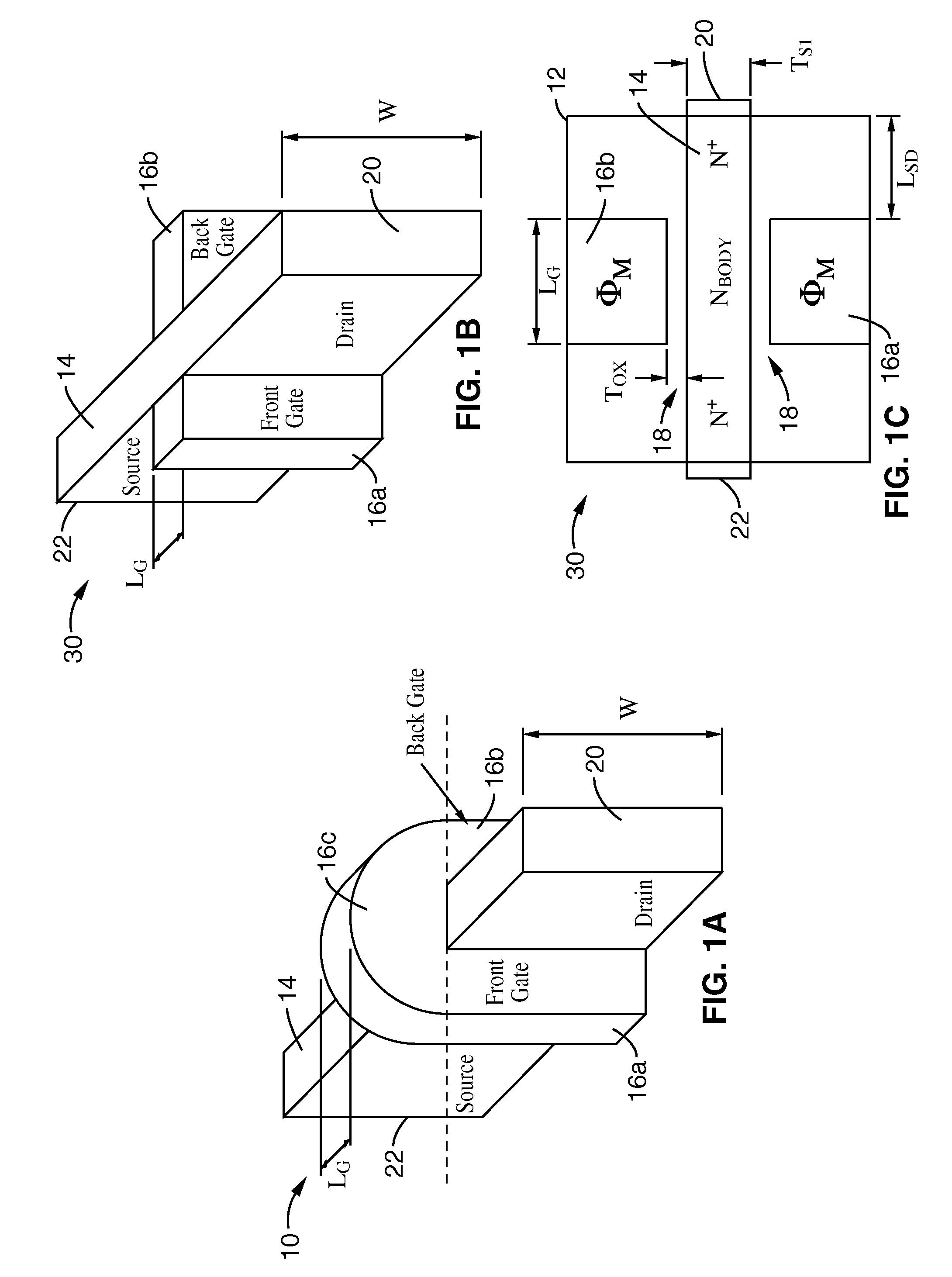
[0096]FIG. 1A through FIG. 1C illustrate views (perspective and top) of FinFET transistor embodiments 10 with a double-gated structure, and 30 adapted with a back-gate structure.

[0097] In the embodiment 10 of FIG. 1A, a fin body 14 is shown making up the transistor channel. A gate 16 overlays the fin, and includes a first side portion 16a, a second side portion 16b and a top portion 16c (above the body of the fin). It should be noted that the gate is shown in a vertical fin configuration which can be of similar dimension to the fin body of the channel. This configuration, having gates on both sides of the channel but which are not electrically separate from one another, is generally referred to as a double-gated FinFET.

[0098] In FIG. 1B, the top gate portion 16c of FIG. 1A has been removed to create the FinFET embodiment 30 configured with separate (i.e., substantially electrically isolated) front-gate 16a and back-gate 16b. FIG. 1C illustrates a top vie...

example 3

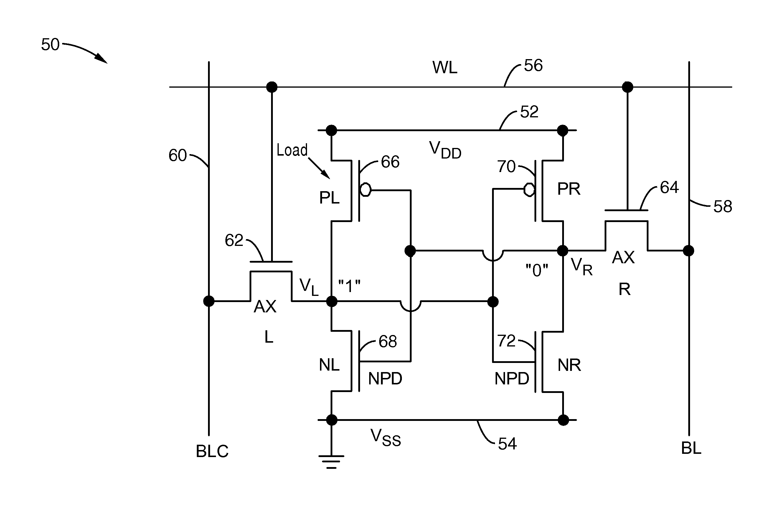
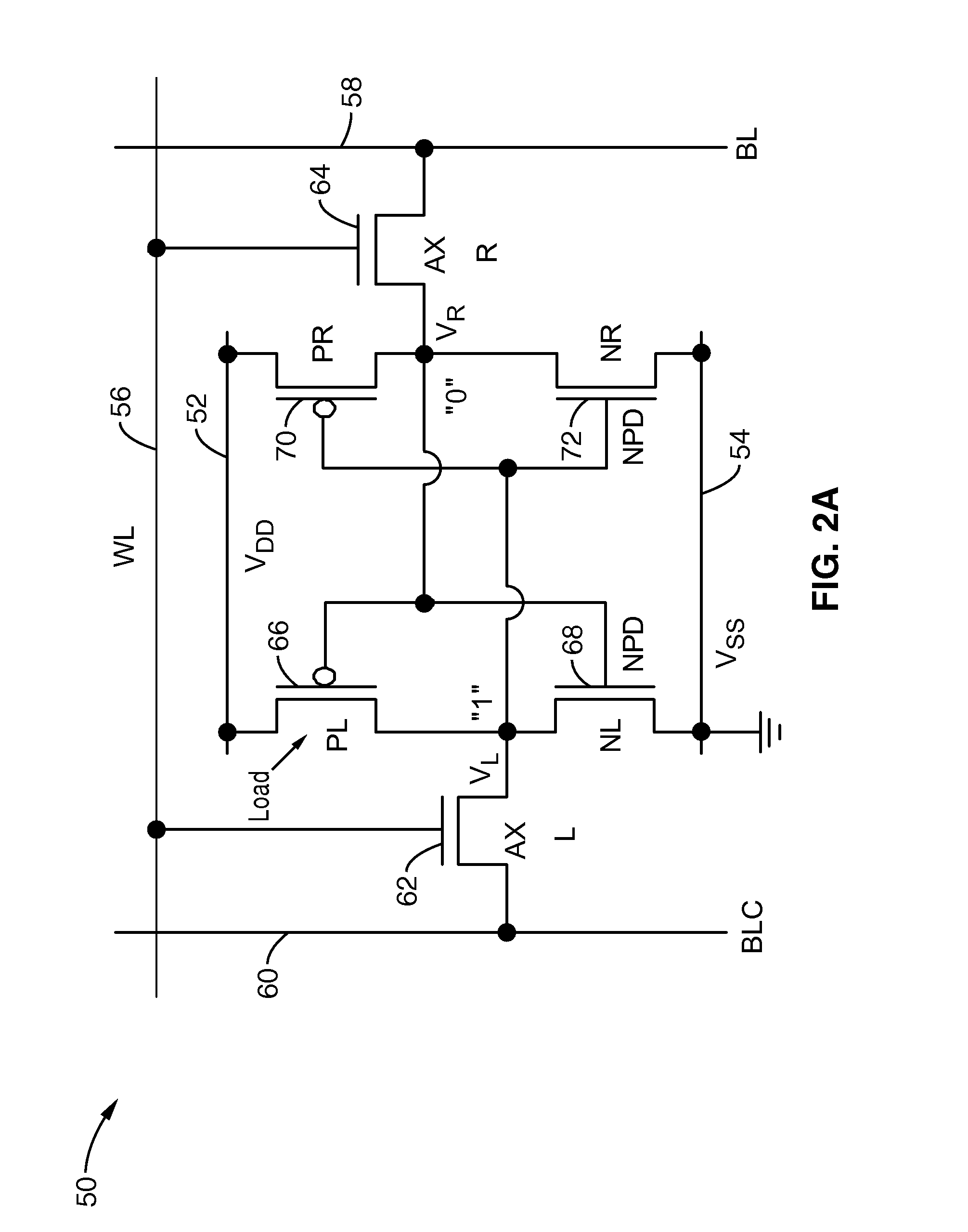
Back-Gated (BG) FinFET 6-T SRAM Cell Designs

[0110] Whereas adaptive body biasing becomes less effective with bulk-Si MOSFET scaling, back-gate biasing of a thin-body MOSFET remains effective for dynamic control of Vt with transistor scaling, and can provide improved control of short-channel effects as well. The strong back-gate biasing effect can thus be leveraged to optimize the performance of FinFET-based SRAMs through a dynamic adjustment of the effective cell β-ratio.

[0111]FIG. 6A illustrates an embodiment 90 of an SRAM memory cell. The power supply is represented as VDD 92 and Vss 94. Signals are represented with a word line 96, bit-line 98, and bit-line complement 100. A first access transistor 102 is on a first side of the memory cell, and a second access transistor 104 is on a second side of the memory cell. The four transistors which form the cross-coupled inverter latch of the memory cell thus comprise transistors 106, 108 on the first side, and transistors 110, 112 on t...

example 4

4-T SRAM Cell with Dynamic Feedback

[0116] Toward providing further reductions in cell area, aspects of the invention include embodiments of 4-T SRAM cell designs. In conventional attempts to create a 4-T SRAM cell design, high-leakage PMOS access transistors are used to compensate for the leakage currents in the pull-down NMOS transistors during standby. Although compensation current is only needed for the “1” storage node, both PMOS access transistors draw currents from the bit-lines, resulting in high power dissipation. Dynamic control of the PMOS threshold voltage (Vtp) according to the present invention offers a means for selectively adjusting the compensation leakage current, and also provides higher effective β-ratio for the 4-T SRAM cell design, thereby making the manufacture of 4-T SRAM cells practical for a number of application areas.

[0117]FIG. 8A and FIG. 8B illustrate an embodiment 130 of a four transistor (4-T) SRAM memory cell. Power is shown as Vss 134, while VDD is...


PUM


Abstract

Intrinsic variations and challenging leakage control in current bulk-Si MOSFETs force undesired tradeoffs to be made and limit the scaling of SRAM circuits. Circuits and mechanisms are taught herein which improve leakage and noise margin in SRAM cells, such as those comprising either six-transistor (6-T) SRAM cell designs, or four-transistor (4-T) SRAM cell designs. The inventive SRAM cells utilize a feedback means coupling a portion of the storage node to a back-gate of an access transistor. Preferably feedback is coupled in this manner to both access transistors. SRAM cells designed with this built-in feedback achieve significant improvements in cell static noise margin (SNM) without area penalty. Use of the feedback scheme also results in the creation of a practical 4-T FinFET-based SRAM cell that achieves sub-100 pA per-cell standby current and offers similar improvements in SNM as the 6-T cell with feedback.

Description

CROSS-REFERENCE TO RELATED APPLICATIONS [0001] This application claims priority from U.S. provisional application Ser. No. 60 / 758,345, filed on Jan. 11, 2006, incorporated herein by reference in its entirety.STATEMENT REGARDING FEDERALLY SPONSORED RESEARCH OR DEVELOPMENT [0002] Not Applicable INCORPORATION-BY-REFERENCE OF MATERIAL SUBMITTED ON A COMPACT DISC [0003] Not Applicable NOTICE OF MATERIAL SUBJECT TO COPYRIGHT PROTECTION [0004] A portion of the material in this patent document is subject to copyright protection under the copyright laws of the United States and of other countries. The owner of the copyright rights has no objection to the facsimile reproduction by anyone of the patent document or the patent disclosure, as it appears in the United States Patent and Trademark Office publicly available file or records, but otherwise reserves all copyright rights whatsoever. The copyright owner does not hereby waive any of its rights to have this patent document maintained in sec...

Claims


Application Information

Patent Timeline
Patent Type & Authority Applications(United States)
IPC IPC(8): G11C11/00
CPCG11C11/412H01L27/11H01L29/785H01L27/1108H01L27/1104H10B10/00H10B10/12H10B10/125
Inventor GUO, ZHENGBALASUBRAMANIAN, SRIRAMZLATANOVICI, RADUKING, TSU-JAENIKOLIC, BORIVOJE
Owner RGT UNIV OF CALIFORNIA
Why Eureka
Try Eureka