Methods for fabricating and filling conductive vias and conductive vias so formed

a technology of conductive vias and conductive materials, which is applied in the direction of semiconductor devices, semiconductor device details, electrical apparatus, etc., can solve the problems of complex processes, shortening between a conductive via and the substrate, and not adhering well to the materials (e.g., silicon) of many substrates, so as to reduce the potential for electrical shorting and facilitate selective growth of conductive materials

Active Publication Date: 2007-08-09
MICRON TECH INC
View PDF9 Cites 74 Cited by
  • Summary
  • Abstract
  • Description
  • Claims
  • Application Information

AI Technical Summary

Benefits of technology

[0011] A method for forming one or more conductive vias includes forming one or more via holes. The via holes may extend fully or partially through a substrate, such as a semiconductor device, an interposer, or another semiconductor device structure. The via holes may be formed with a single mask, eliminating the potential for misalignment between different sections of a via hole, which are formed through layers of different materials. The via holes may be formed or subsequently processed in such a way as to facilitate adhesion of materials that are subsequently introduced therein to the surfaces thereof. Such processing may include providing via hole surfaces with roughened features or other features that enhance the surface areas thereof.
[0013] The dielectric coating may be formed in such a way as to extend onto an edge of a bond pad that is continuous with a via hole, thereby reducing the potential for electrical shorting between a subsequently fabricated conductive via and the material of the substrate through which the conductive via extends.
[0014] A layer or film of barrier material may also be formed over the surfaces of each via hole. By way of example only, the barrier material may prevent interdiffusion between a conductive material and the material of an insulative coating or of the substrate through which the via hole extends.
[0015] Conductive material may be introduced into the via hole by a variety of processes. For example, a seed material coating or other “base layer” may be formed and, if necessary, patterned to remove seed material from undesired regions of a semiconductor device structure (e.g., the major surfaces of the semiconductor device structure). The seed material facilitates selective growth of conductive material at desired locations, such as over the surfaces of each via hole. Thus, once the seed material coating covers only desired portions of a semiconductor device structure, the conductive material may be selectively introduced into the via holes and over any other desired locations of the semiconductor device structure (e.g., on a bond pad through which a via hole extends and with which the conductive via will communicate).

Problems solved by technology

Although these and similar materials may be used to form very thin insulative coatings on the surfaces of via holes, they do not adhere well to the materials (e.g., silicon) of many substrates through which via holes are formed or to the conductive materials that are subsequently introduced into the via holes to form an electrically conductive via.
The low adhesion of such dielectric materials, as well the potential for misalignment when multiple masks are used to form and passivate via holes may result in shorting between a conductive via and the substrate through which the conductive via extends.
In addition, some of the processes that are currently used to fabricate conductive vias are complex, require expensive materials or equipment that is not widely used in semiconductor device fabrication processes, or are otherwise undesirable.

Method used


Image

  • Methods for fabricating and filling conductive vias and conductive vias so formed
  • Methods for fabricating and filling conductive vias and conductive vias so formed
  • Methods for fabricating and filling conductive vias and conductive vias so formed

Examples


example 1

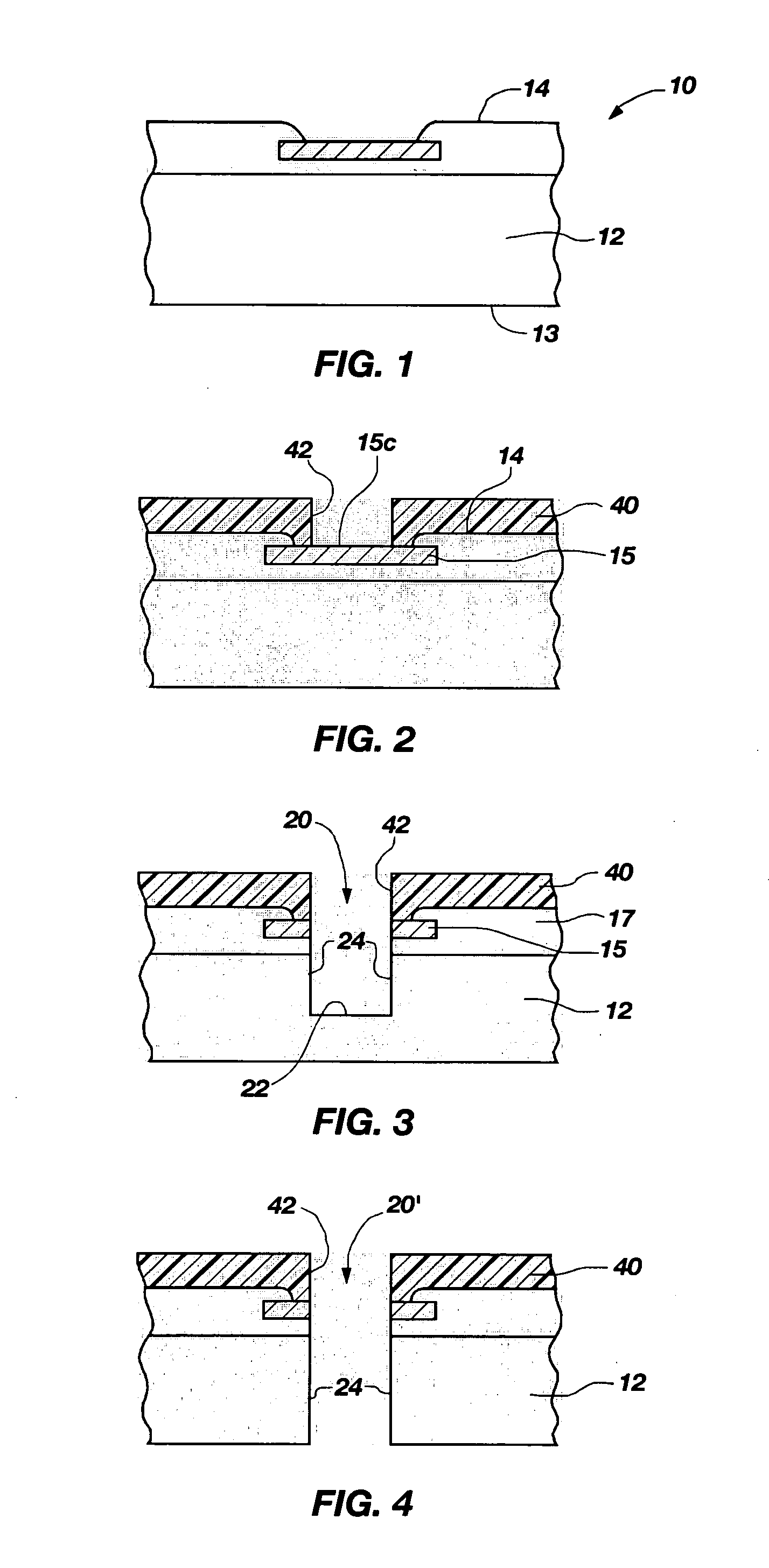
[0086] With reference to FIGS. 21 through 27, an example of a process that may be used to form via holes 20 in a substrate 12 and insulate, or passivate, surfaces 24 thereof is described.

[0087] In FIG. 21, a via hole 20 is formed in substrate 12. While via hole 20 is depicted as extending only partially through substrate 12 and is, thus, known in the art as a “blind via hole,” via hole 20 may alternatively extend completely through substrate 12. Via hole 20 may be formed by any suitable process, including, without limitation, by use of a mask through which one or more etchants selectively remove material of substrate 12, by laser ablation techniques, or otherwise, as known in the art.

[0088] While FIGS. 21 through 27 depict the process of EXAMPLE 1 as being useful for forming conductive vias that extend through “blind” areas of substrate 12, which do not include integrated circuitry or bond pads, these processes may also be used to form conductive vias that extend through bond pads...

example 2

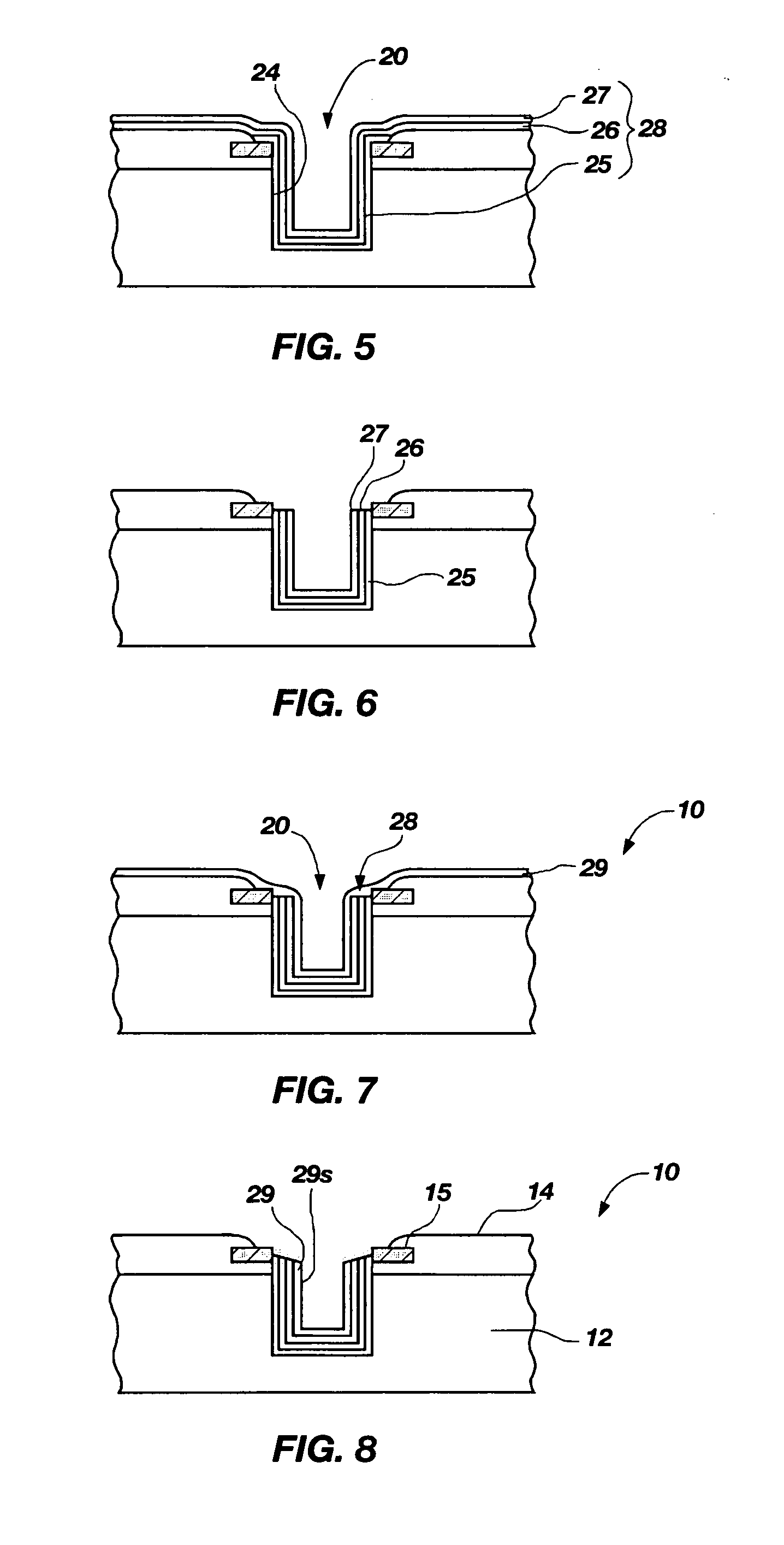
[0097]FIGS. 28 through 35 illustrate another example of a process that may be used to form via holes 20 in a substrate 12 and insulate, or passivate, surfaces 24 of via holes 20.

[0098] In FIG. 28, a via hole 20 is formed in substrate 12.

[0099] As shown in FIG. 29, a first adhesion layer 25 is formed on surface 24 of via hole 20 and on an active surface. 14 of substrate 12. Portions of first adhesion layer 25 that overlie active surface 14 of substrate 12 are then immediately removed, as shown in FIG. 30.

[0100] Next, as illustrated in FIG. 31, a layer 26 comprising low-K dielectric material is deposited over remaining portions of first adhesion layer 25 and over active surface 14. Thereafter, portions of dielectric layer 26 that overlie active surface 14 are removed, as depicted in FIG. 32.

[0101] A second adhesion layer 27 is then formed, as shown in FIG. 33. Portions of second adhesion layer 27 that overlie active surface 14 are subsequently removed, while portions of second adh...

example 3

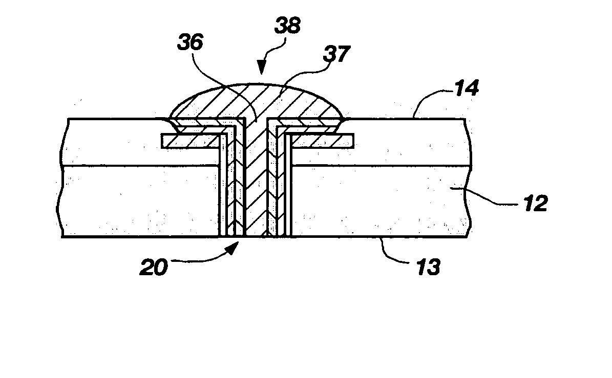
[0104] In another exemplary via hole formation and insulation technique, which builds upon the process flow described in EXAMPLES 1 and 2, the first adhesion layer may be omitted and replaced with a process for roughening surface 24 of via hole 20, as shown in FIG. 36. Surface 24 may be roughened, for example, by the process or processes that are used to form via hole 20. Alternatively, a separate etch process may be used to increase the roughness of surface 24. The roughness of surface 24 enhances the direct adhesion of dielectric layer 26 or dielectric coating 28 to the material of substrate 12 at surface 24, as shown in FIG. 37.


PUM

PropertyMeasurementUnit
aspect ratiosaaaaaaaaaa
dielectric constantaaaaaaaaaa
aspect ratioaaaaaaaaaa

Abstract

Methods for forming conductive vias include forming one or more via holes in a substrate. The via holes may be formed with a single mask, with the protective layers, bond pads, or other features of the substrate acting as hard masks in the event that a photomask is removed during etching processes. The via holes may be configured to facilitate adhesion of a dielectric coating that includes a low-K dielectric material to the surfaces thereof. A barrier layer may be formed over surfaces of each via hole. A base layer, which may comprise a seed material, may be formed to facilitate the subsequent, selective deposition of conductive material over the surfaces of the via hole. The resulting semiconductor devices, intermediate structures, and assemblies and electronic devices that include the semiconductor devices that result from these methods are also disclosed.

Description

BACKGROUND OF THE INVENTION [0001] 1. Field of the Invention [0002] The present invention relates generally to techniques for forming conductive vias of semiconductor device components and, more specifically, to conductive via-forming techniques in which conductive material is selectively deposited on the surfaces of a via hole without being deposited on the major surfaces of the semiconductor device component through which the via extends. The present invention also relates to conductive vias with selectively deposited conductive layers, as well as to semiconductor device components that include the conductive vias and semiconductor device assemblies that include the semiconductor device components. [0003] 2. Background of Related Art [0004] The parallel trends of ever-decreasing size and ever-increasing ability in the electronics industry have driven a need for semiconductor devices, semiconductor device assemblies, and semiconductor device packages of ever-decreasing size and eve...

Claims


Application Information

Patent Timeline
Patent Type & Authority Applications(United States)
IPC IPC(8): H01L21/44
CPCH01L21/76898H01L23/481H01L2224/16H01L2224/13009H01L2924/09701H01L2224/05009H01L2224/13025H01L2224/05568H01L2224/05001H01L2224/16145H01L2224/17181H01L2224/05076H01L24/05H01L24/03H01L21/768H01L21/28H01L21/44
Inventor AKRAM, SALMANHIATT, WILLIAM MARKOLIVER, STEVEWOOD, ALAN G.RIGG, SIDNEY B.WARK, JAMES M.KIRBY, KYLE K.
Owner MICRON TECH INC
Why Eureka
Try Eureka