Structure, electron emitting device, secondary battery, electron source, and image display device

a technology of electron emitting device and electron source, which is applied in the direction of discharge tube luminescnet screen, cell components, and discharge tube with screen, etc., can solve the problems of electron emission characteristics that are not stable, and achieve the effect of reducing the thickness of the oxide film formed

Inactive Publication Date: 2007-08-16
CANON KK
View PDF50 Cites 24 Cited by
  • Summary
  • Abstract
  • Description
  • Claims
  • Application Information

AI Technical Summary

Benefits of technology

[0008] However, in the Japanese Unexamined Patent Publication No. 11-139815, the metal having catalytic particles dispersed therein and the substrate of Si are subjected to a process for growing carbon fibers and hence have an oxide film easily formed on their surfaces. Since silicon oxide is an insulating material, when the oxide film becomes thick, the oxide film sometimes prevents the electric connection between the metal and the substrate and the carbon fibers. In addition to Si, an oxide material of an element having an electron configuration of atom having no d-orbital electron such as Al is an insulating material, so that when this material is used as the material of the supporting member of the carbon fibers, it is necessary to reduce the thickness of an oxide film formed on the surface of the supporting member.

Problems solved by technology

Moreover, when a material including TiN, ZrN, TaN, or NbN is used as the supporting member of the carbon fibers as disclosed in the Japanese Unexamined Patent Publication No. 2002-289087, there are cases where the following problems occur.
Therefore, when the composition ratio of elements constituting the alloy varies from an initial desired state, the formed carbon fibers also vary in diameter, length, crystalline structure, and the like, which sometimes causes problems of degradation and variations in electron emission characteristics.

Method used


Image

  • Structure, electron emitting device, secondary battery, electron source, and image display device
  • Structure, electron emitting device, secondary battery, electron source, and image display device
  • Structure, electron emitting device, secondary battery, electron source, and image display device

Examples


example 1

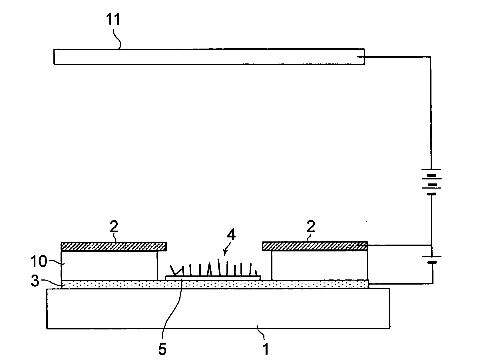
[0116] In FIG. 3A is shown a view, when viewed from above, of an electron emitting device manufactured according to the present example and FIG. 3B is a sectional view taken on a line A-A in FIG. 3A.

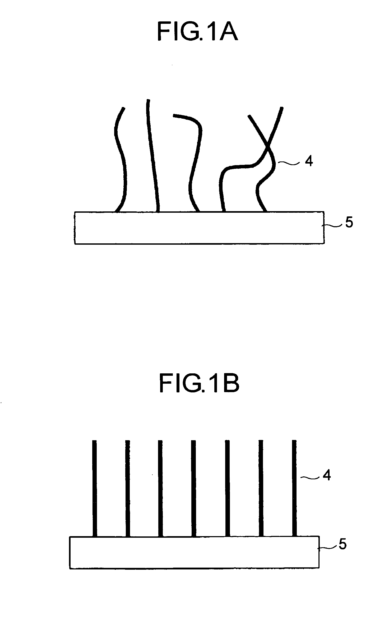
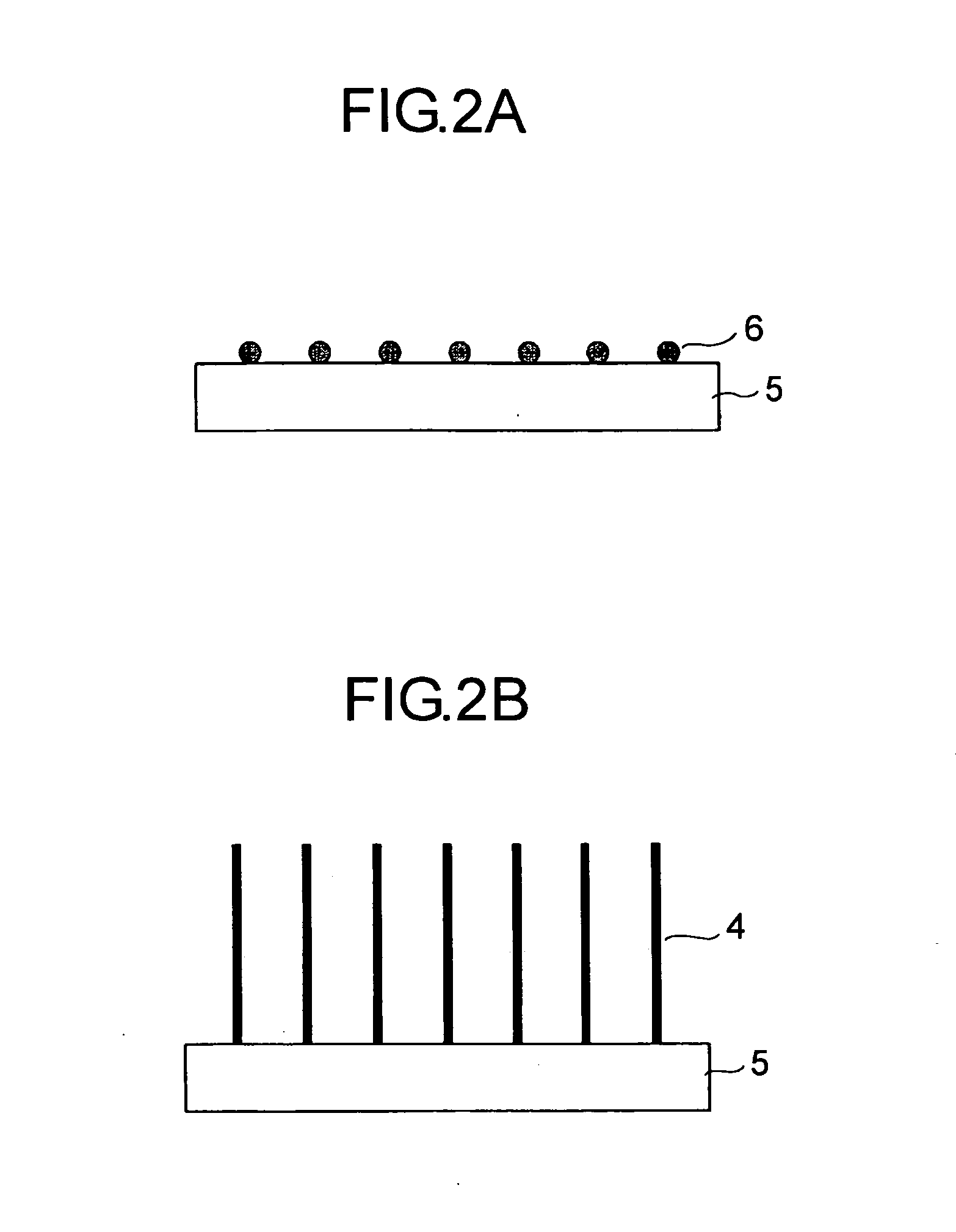
[0117] In FIG. 3A and FIG. 3B, a reference numeral 1 denotes the insulating substrate, 2 denotes the control electrode (also referred to as a drawing-out electrode, or a gate electrode), 3 denotes the electrode (referred to as a cathode electrode), 4 denotes the plurality of carbon fibers, 5 denotes the conductive member made of a member material of the present invention.

[0118] The manufacturing process of the electron emitting device of the present example will be described by the use of FIG. 7.

(Step 1: refer to FIG. 7A)

[0119] A quartz substrate was used as a substrate 1. The substrate 1 was sufficiently cleaned and then Ti and Pt were vapor-deposited continuously in layer thicknesses of 5 nm (not shown) and 30 nm, respectively, on the substrate 1 by a sputtering method. Next, a re...

example 2

[0132] The construction of an electron emitting device according to an example 2 of the present invention is shown in FIG. 4A and FIG. 4B. Hereinafter, the differences in the manufacturing method between the example 1 and the example 2 will be described.

[0133] In the present example, in the step 1, the electrode 3 was formed in a thickness of 500 nm and the control electrode 2 was formed in a thickness of 30 nm. Moreover, in the step 2, Zr7Al3 was used as a target for sputtering. An analysis of the member 5 (ZrxAl(1−x)N (x3 was used a catalyst produced by adding approximately 20 atm % Co to metal Pd.

[0134] Even in the member 5 (ZrxAl(1−x)N (x4, which showed that a contact layer was stably formed. Moreover, the carbon fibers 4 could be stably grown by the alloyed catalyst.

example 3

[0135] The construction of an electron emitting device according to an example 3 of the present invention is shown in FIG. 5A and FIG. 5B. Hereinafter, the differences in the manufacturing method between the example 1 and the example 3 will be described.

[0136] In the present example, in the step 4, the member 5 and the metallic catalyst particles 6 were formed across the electrode 3 and the gap between the electrode 3 and the control electrode 2. The member 5 was formed nearly to a middle position (approximately half of the gap) between the electrode 3 and the control electrode 2. Moreover, in the present example, in the step 2, a target made of NbC (niobium carbide) was used as a target. An analysis of the member 5 (NbxC(1−x)N (x3, a catalyst produced by adding approximately 10 atm % Fe to metal Pd was used. Furthermore, in the step 5, 0.1% acetylene diluted with nitrogen was used as a gas for growing the carbon fibers.

[0137] Even in the member 5 (NbxC(1−x)N) of the present examp...


PUM

PropertyMeasurementUnit
diameteraaaaaaaaaa
diameteraaaaaaaaaa
diameteraaaaaaaaaa

Abstract

The present invention prevents the oxidization of a member of carbon fibers and improves the electric connection between the carbon fibers and the member of carbon fibers. In the present invention, a member 5 of carbon fibers 4 includes: a first element selected from the group consisting of IVa group elements and Va group elements; a second element selected from the group consisting of C, Al, Si, Cr, and Zr; and N. Preferably, the first element is Ti. More preferably, the member 5 includes Al or Si and the ratio of Al or Si to Ti is not less than 10 atm % and not more than 30 atm %.

Description

BACKGROUND OF THE INVENTION [0001] 1. Field of the Invention [0002] The present invention relates to a structure, an electron emitting device, a secondary battery, an electron source, and an image display device each of which uses carbon fibers. [0003] 2. Description of the Related Art [0004] In recent years, field emission type electron emitting devices include an electron emitting device using carbon fibers as electron emitting bodies. Because of such a field enhancement effect resulting from shape that is produced by using carbon fibers as electron emitting bodies, the electron emitting device using carbon fibers as electron emitting bodies can emit electrons from the electron emitting bodies in a lower electric field intensity than an electron emitting body made of carbon or the like shaped like a film (in the shape of a plane). [0005] Methods for forming carbon fibers used for electron emitting bodies include a method for applying carbon fibers prepared in advance to the surfac...

Claims


Application Information

Patent Timeline
Patent Type & Authority Applications(United States)
IPC IPC(8): H01J1/02B82B1/00B82Y30/00B82Y99/00C01B31/02H01J1/304H01J9/02H01J29/04H01J31/12H01M4/133H01M4/1393H01M4/587H01M4/88
CPCB82Y10/00H01J9/025Y02E60/122H01J29/481H01J2201/30469H01J29/04
Inventor TSUKAMOTO, TAKEOKITAMURA, SHINKUBOTA, OICHI
Owner CANON KK
Why Eureka
Try Eureka