High gain, high frequency CMOS oscillator circuit and method

Active Publication Date: 2007-08-16
MONTEREY RES LLC
View PDF6 Cites 16 Cited by
  • Summary
  • Abstract
  • Description
  • Claims
  • Application Information

AI Technical Summary

Benefits of technology

[0011] In order to place the gate terminals of the first and second transistors at an optimal bias voltage, a current-controlled biasing circuit can be used. The biasing circuit, as one example, can include a current source and a diode-coupled transistor. The DC bias voltage thus generated across the diode-connected transistor can be connected to gate termination of a gain element through a high impedance path. The high imp

Problems solved by technology

High start-up gain can reduce the start-up time (Too high a gain is also not desirable, as defined by

Method used


Image

  • High gain, high frequency CMOS oscillator circuit and method
  • High gain, high frequency CMOS oscillator circuit and method
  • High gain, high frequency CMOS oscillator circuit and method

Examples


Embodiment Construction

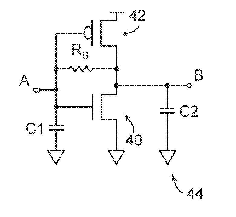
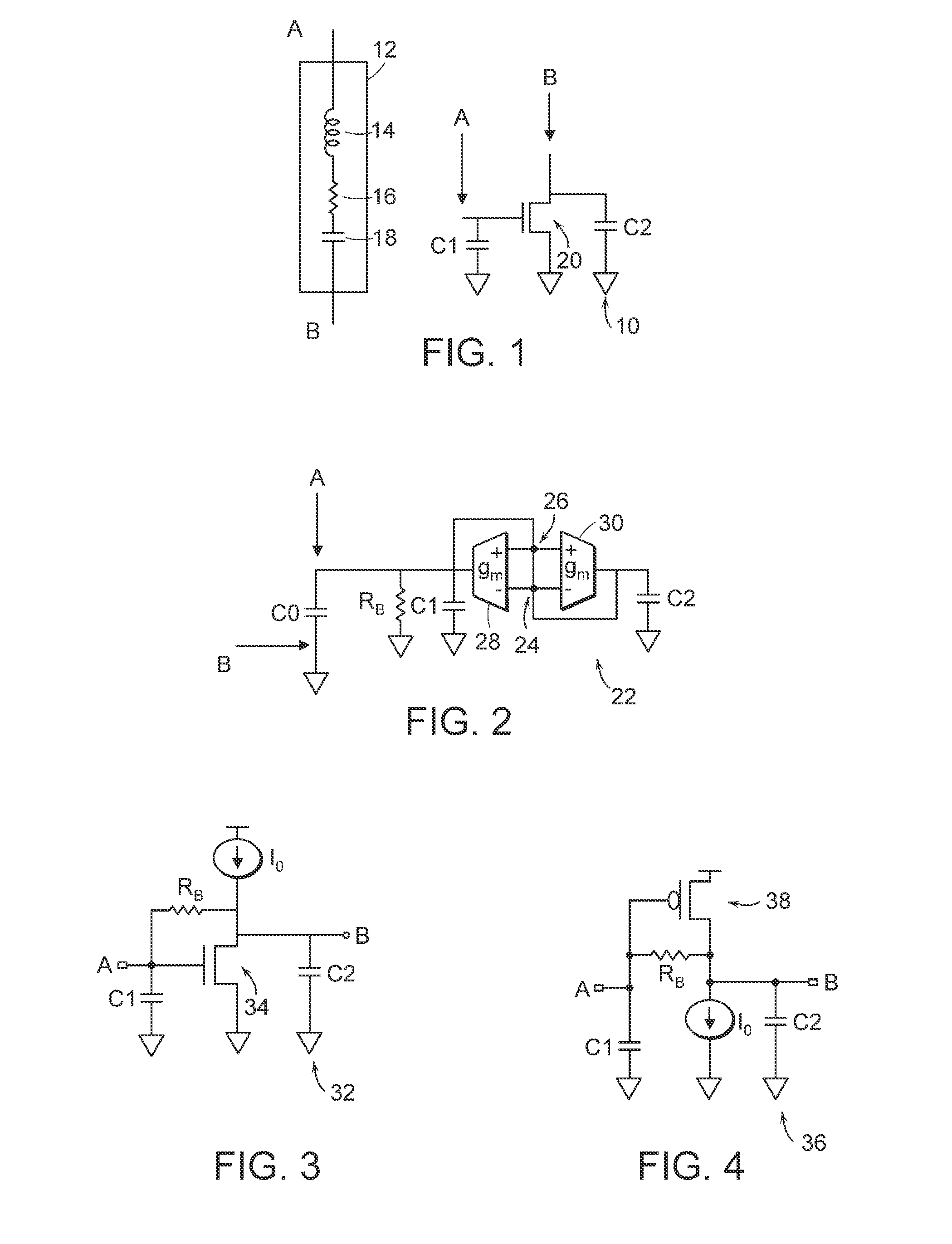
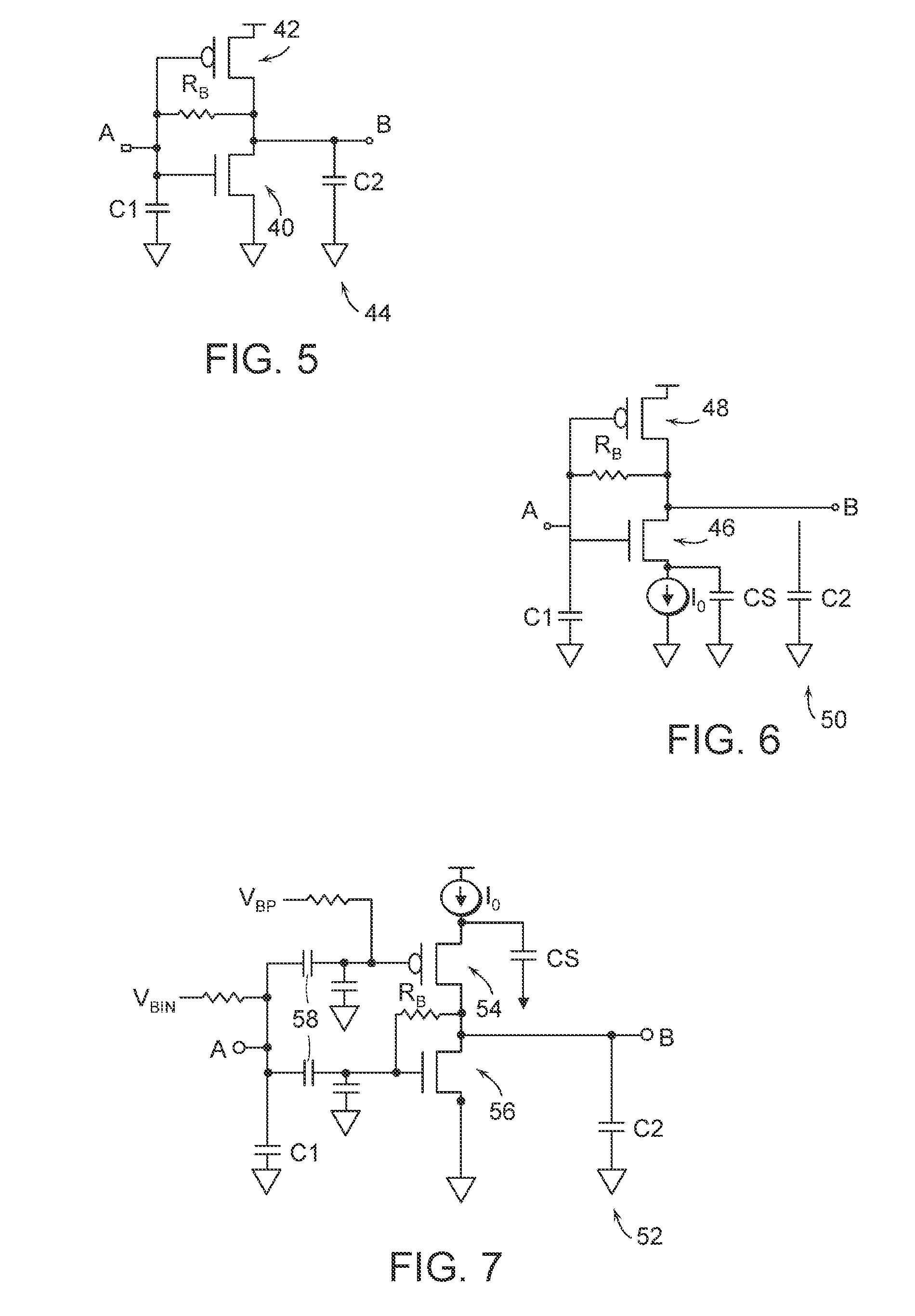
[0032] Turning now to the drawings, FIG. 1 illustrates one form of active circuitry 10 used to initiate and amplify output of a resonator, such as a piezoelectric resonator including, but not limited to, a crystal or SAW. A resonator 12 can be coupled across two pins labeled A and B. Resonator 12 is shown as a model of a piezoelectric resonator or SAW. Resonator 12 can be realized as an inductor 14, resistor 16, and capacitor 18.

[0033] Active circuit 10 is used to generate an active impedance ZA. The active impedance ZA has both an imaginary (ZI) and real resistance (ZR); however, the real resistance is a negative value. For reliable start-up conditions, the value of this negative real resistance should be approximately three times larger than resonator 12 motional resistance.

[0034] Within active circuit 10 are two capacitors C1 and C2. The resonance frequency produced by circuit 10 can be trimmed by implementing capacitors C1 and C2 as capacitor banks switched by pass gates, for ...


PUM


Abstract

An oscillator amplifier circuit is provided. The amplifier circuit can be used with a resonator to amplify and form a resonating oscillator. The amplifier circuit comprises an active circuit which includes an inverter and a current-controlled biasing circuit. One transistor of the inverter receives a voltage produced from the biasing circuit in order to place a gate terminal of that transistor at approximately a threshold voltage. The other transistor can be biased using a passive circuit element, such as a resistor. Therefore, both transistors are biased independent of each other within the optimal gain region. Large shunt capacitors are not required and the total current consumption is controlled through a variable resistor coupled to the source terminal of either the first transistor, second transistor, or possibly both transistors of the inverter to adjust the amplitude of the oscillating output.

Description

BACKGROUND OF THE INVENTION [0001] 1. Field of the Invention [0002] The present invention relates to an electronic circuit or subsystem and, more particularly, to an electronic oscillator that uses biasing voltages to maintain complementary metal oxide semiconductor (CMOS) transistors in a relatively low power consumptive state while achieving increased gain at higher frequencies of operation. [0003] 2. Description of the Related Art [0004] The following descriptions and examples are not admitted to be prior art or conventional by virtue of their inclusion within this section. [0005] Within nearly every electronic subsystem is some form of generator that produces cyclical waveforms. The waveform generator is oftentimes referred to as an oscillator. Depending on the application, an oscillator can be used to source regularly spaced pulses or clock signals. Oscillators are oftentimes rated depending on their stability and accuracy, frequency adjustability (i.e., tunability), gain of ac...

Claims


Application Information

Patent Timeline
IPC IPC(8): H03L7/099
CPCH03B2200/0062H03B5/364
Inventor MAHESHWARI, SANJEEV KUMAR
Owner MONTEREY RES LLC
Why Eureka
Try Eureka