
Apparatus for manufacturing semiconductor devices

a semiconductor device and apparatus technology, applied in the direction of positive displacement liquid engines, separation processes, instruments, etc., can solve the problems of increasing maintenance and repair costs, essentially impossible to precisely control the exhaust pressure, etc., and achieve the effect of reducing the number of apparatus components, effectively exhausted from the system, and stable exhaust pressur

Inactive Publication Date: 2007-08-16
SAMSUNG ELECTRONICS CO LTD
View PDF4 Cites 5 Cited by
  • Summary
  • Abstract
  • Description
  • Claims
  • Application Information

AI Technical Summary

Benefits of technology

[0009]Accordingly, the present invention provides an exhaust system apparatus for manufacturing semiconductor devices, which can effectively exhaust the exhaust materials from the manufacturing operations.
[0010]The present invention also provides an exhaust system apparatus for manufacturing semiconductor devices, which can reduce the maintenance and repair costs and also reduce lost time and inconvenience.
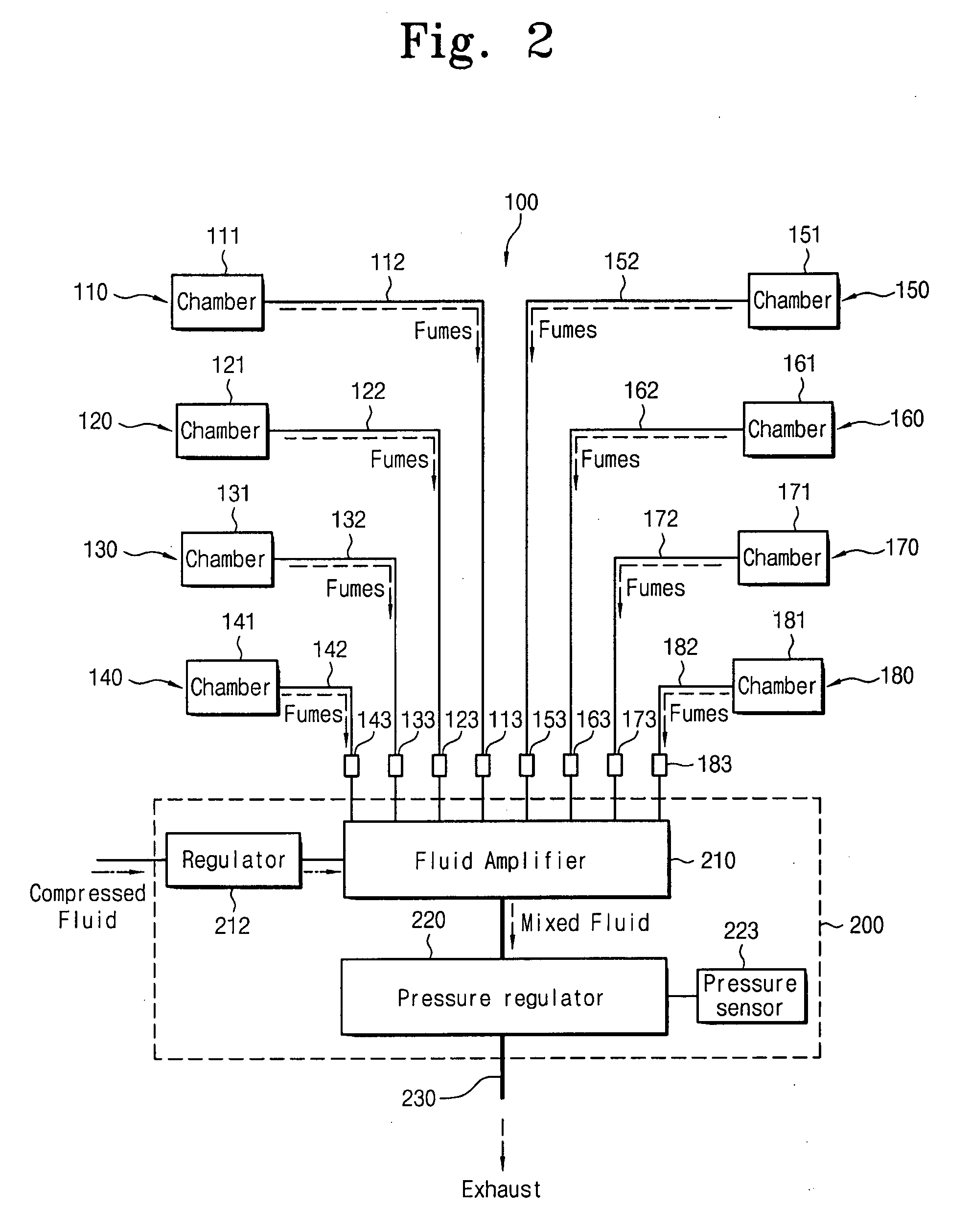
[0019]In some embodiments, the pressure sensors may advantageously be closer to the fluid amplifier than to the respective chambers. The fluid amplifier may use the Coanda effect through the introduction of the compressed fluid to amplify the exhaust effect and to assist with introducing the exhaust material(s). The compressed fluid used for this purpose may include pressurized air or nitrogen gas.
[0020]According to the present invention, since an exhaust system using the air-amplifying phenomenon as discussed uniformly maintains the exhaust pressure, the exhaust material(s) can be stably and effectively exhausted from the system. Furthermore, because the number of apparatus components can be reduced in accordance with this invention, the maintenance and repair costs can also be reduced.

Problems solved by technology

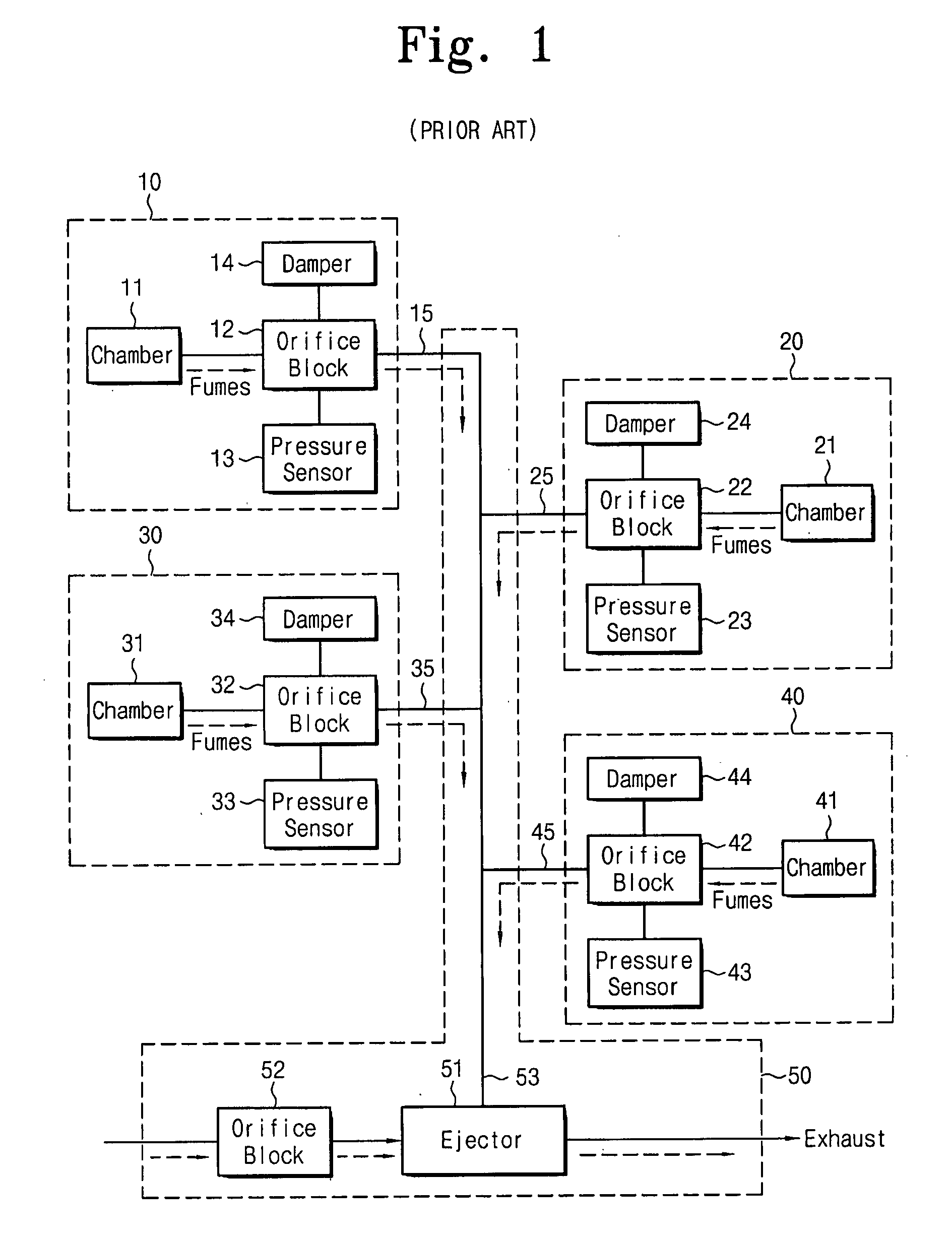
However, when any of the orifice blocks 12, 22, 32, and 42 becomes blocked by the exhaust material, it becomes essentially impossible to precisely control the exhaust pressure.
Moreover, due to the relatively complicated structure of such an apparatus for exhausting the exhaust materials, the maintenance and repair costs increase as well as the time lost and resulting inconvenience.

Method used


Image

  • Apparatus for manufacturing semiconductor devices
  • Apparatus for manufacturing semiconductor devices
  • Apparatus for manufacturing semiconductor devices

Examples


Embodiment Construction

[0026]Preferred embodiments of the present invention will be described below in more detail with reference to the accompanying drawings. The present invention may, however, be embodied in different forms and should not be construed as limited to the embodiments set forth herein. Rather, these embodiments are provided so that this disclosure will be thorough and complete, and will fully convey the scope of the present invention to those skilled in the art.

[0027]Hereinafter, an exemplary embodiment of the present invention will be described in conjunction with the accompanying drawings.

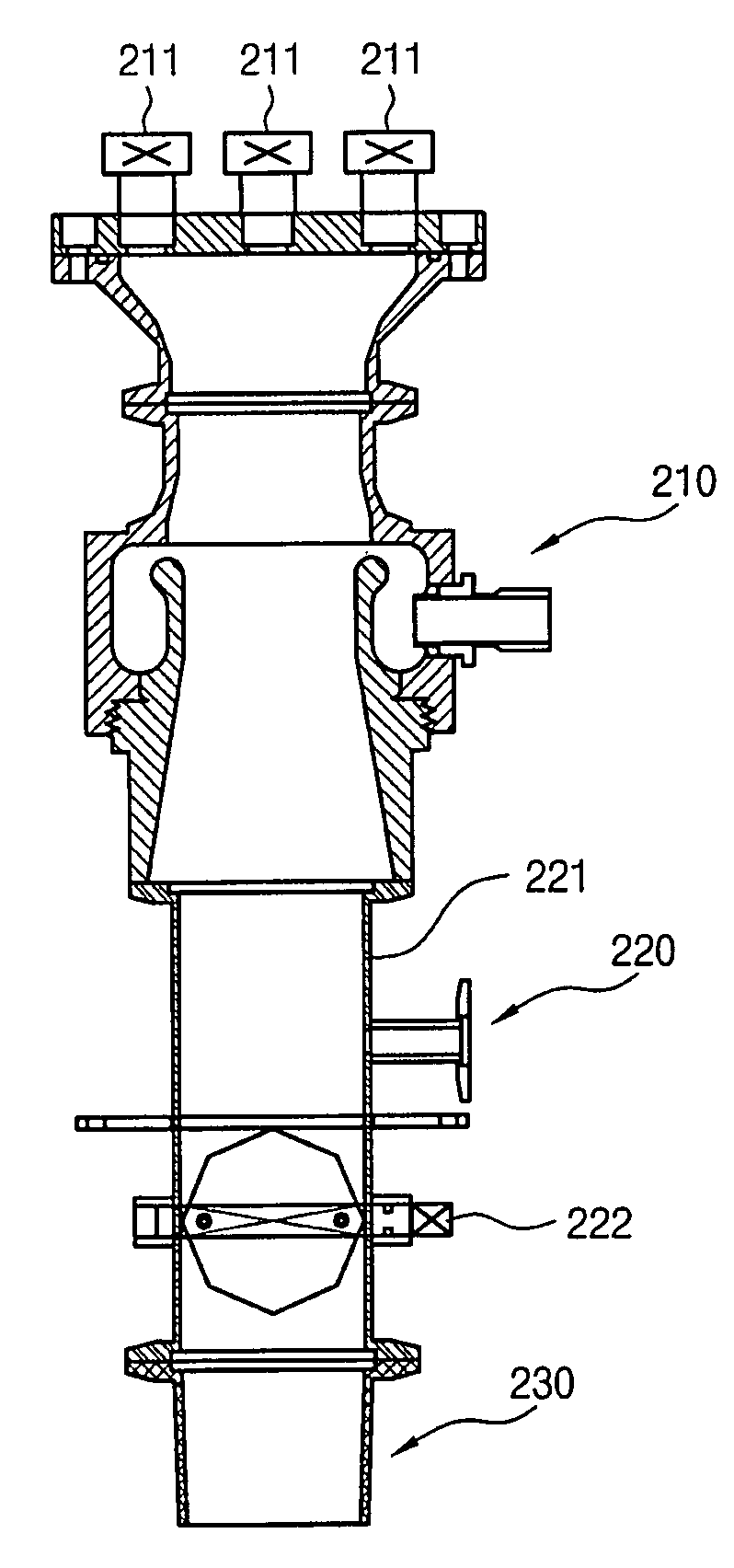
[0028]FIG. 2 is a schematic view of an exhaust system apparatus for manufacturing semiconductor devices according to an embodiment of the present invention; FIG. 3 is an enlarged schematic sectional view of an exhaust module component of the apparatus of FIG. 2; and FIG. 4 is an enlarged schematic sectional view of a fluid amplifier illustrating a Coanda effect in connection with the apparatus of FIG. 2...


PUM

PropertyMeasurementUnit
Pressureaaaaaaaaaa

Abstract

Provided are apparatus and methods for manufacturing semiconductor devices and more specifically exhaust system apparatus and methods used in conjunction with a plurality of semiconductor processing chambers. The overall apparatus includes a plurality of process modules in which a semiconductor process is performed and an exhaust module to which the process modules are independently connected by fluid exhaust lines. The exhaust module amplifies an exhaust functionality of the system by more effectively and reliably drawing exhaust material from the process modules to be efficiently and effectively exhausted from the system.

Description

CROSS-REFERENCE TO RELATED APPLICATIONS[0001]This U.S. non-provisional patent application claims priority under 35 U.S.C. §119 of Korean Patent Application No. 2006-13187, filed on Feb. 10, 2006, the entire contents of which are hereby incorporated by reference.BACKGROUND OF THE INVENTION[0002]The present invention disclosed herein relates to an exhaust system apparatus used in connection with manufacturing semiconductor devices, and more particularly, to an exhaust system apparatus for manufacturing semiconductor devices which demonstrates improved functionality, reliability, and performance.[0003]Generally, an apparatus for manufacturing semiconductor devices processes a wafer under a variety of environments and process conditions. That is, the apparatus for manufacturing semiconductor devices processes the wafer by repeating a variety of unit processes such as a photolithograph, diffusing, etching, chemical vapor deposition, physical vapor deposition, and other such fabrication p...

Claims


Application Information

Patent Timeline
IPC IPC(8): G11C7/00
CPCB08B15/002B01D35/18F16K31/18B01D2201/31
Inventor YOUN, SUNG-CHUL
Owner SAMSUNG ELECTRONICS CO LTD
Learn More