Low resistance gate for power mosfet applications and method of manufacture

a technology of low resistance gate and power mosfet, which is applied in the direction of basic electric elements, electrical apparatus, and semiconductor devices, can solve the problems of significant increase in esr, potential reliability problems, and adversely affecting switching speed

Active Publication Date: 2007-08-16
SEMICON COMPONENTS IND LLC +1
View PDF10 Cites 98 Cited by
  • Summary
  • Abstract
  • Description
  • Claims
  • Application Information

AI Technical Summary

Benefits of technology

[0006]In accordance with one embodiment of the invention, a trench gate field effect transistor is formed as follows. A trench is formed in a semiconductor region, followed by a dielectric layer lining sidewalls and bottom of the trench and extending over mesa regions adjacent the trench. A conductive seed layer is formed in a bottom portion of the trench over the dielectric layer. A low resistance material is grown over the conductive seed layer, wherein the low resistance material is selective to the conductive seed layer.

Problems solved by technology

However, as the devices are scaled down, the gate line-width gets narrower and the sheet resistance contribution to the equivalent series resistance (ESR) increases, adversely affecting the switching speed.
However, current doping concentrations are at saturation levels and any higher levels can result in dopant penetration into the channel region depending on the gate oxide integrity and the thermal budget of the process.
This coupled with the continued trend of shrinking cell pitch and diminishing cross sectional area of gate electrode has resulted in a significant increase in ESR as well as potential reliability issues.
Another challenge in design of power devices, in particular trench MOSFETs, has been forming reliable and low resistance contacts to source and well regions through source contact openings (sometimes formed by recessing silicon mesa) with increasingly high aspect ratios.
The limitations of the manufacturing tools and the process technology, make it difficult to form reliable and low resistance contacts through high aspect ratio source contact openings.

Method used


Image

  • Low resistance gate for power mosfet applications and method of manufacture
  • Low resistance gate for power mosfet applications and method of manufacture
  • Low resistance gate for power mosfet applications and method of manufacture

Examples


Embodiment Construction

[0030]In accordance with the present invention, various techniques for obtaining a low resistance gate in such devices a trench power MOSFETs with the flexibility to use a variety of low resistance materials and / or combinations thereof are described herein. Also, efficient methods for filling high aspect ratio features in devices are described.

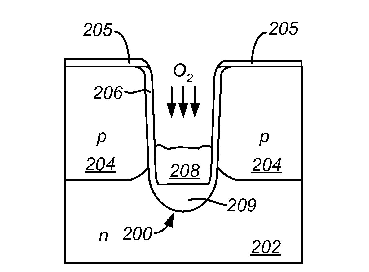
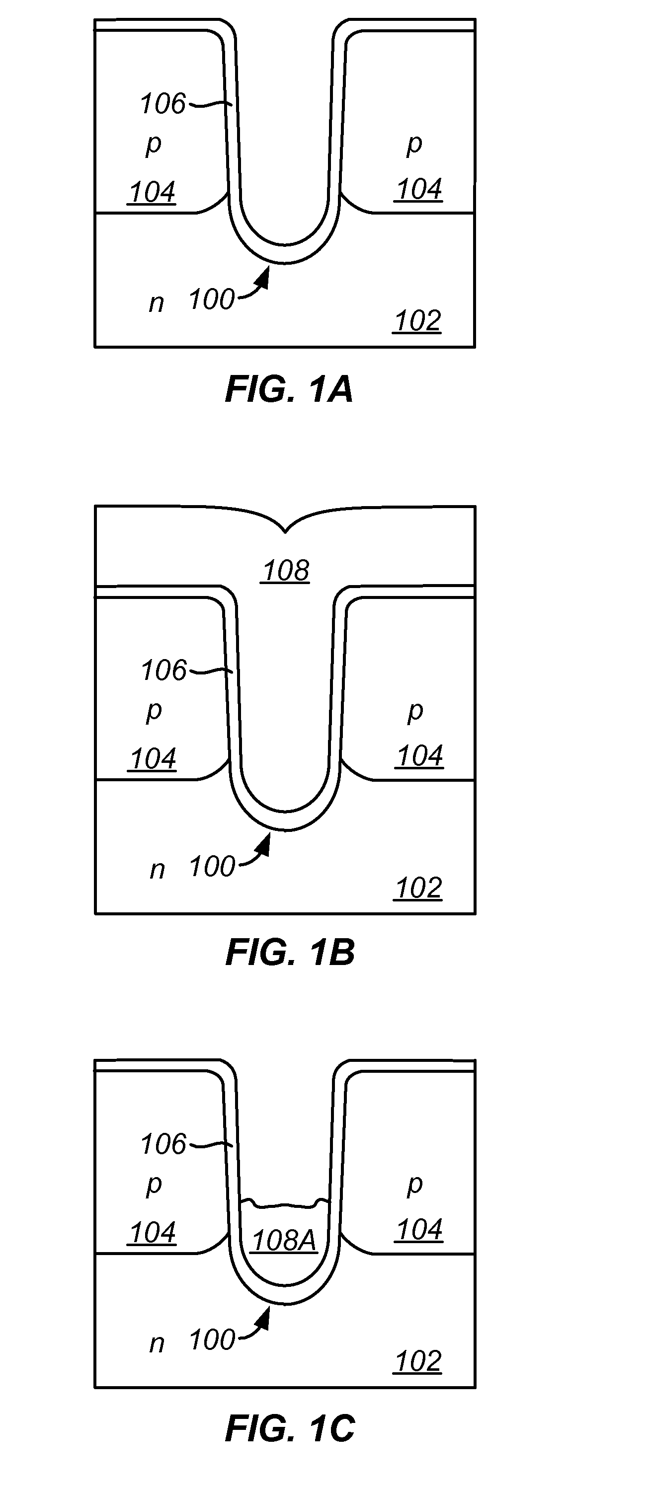
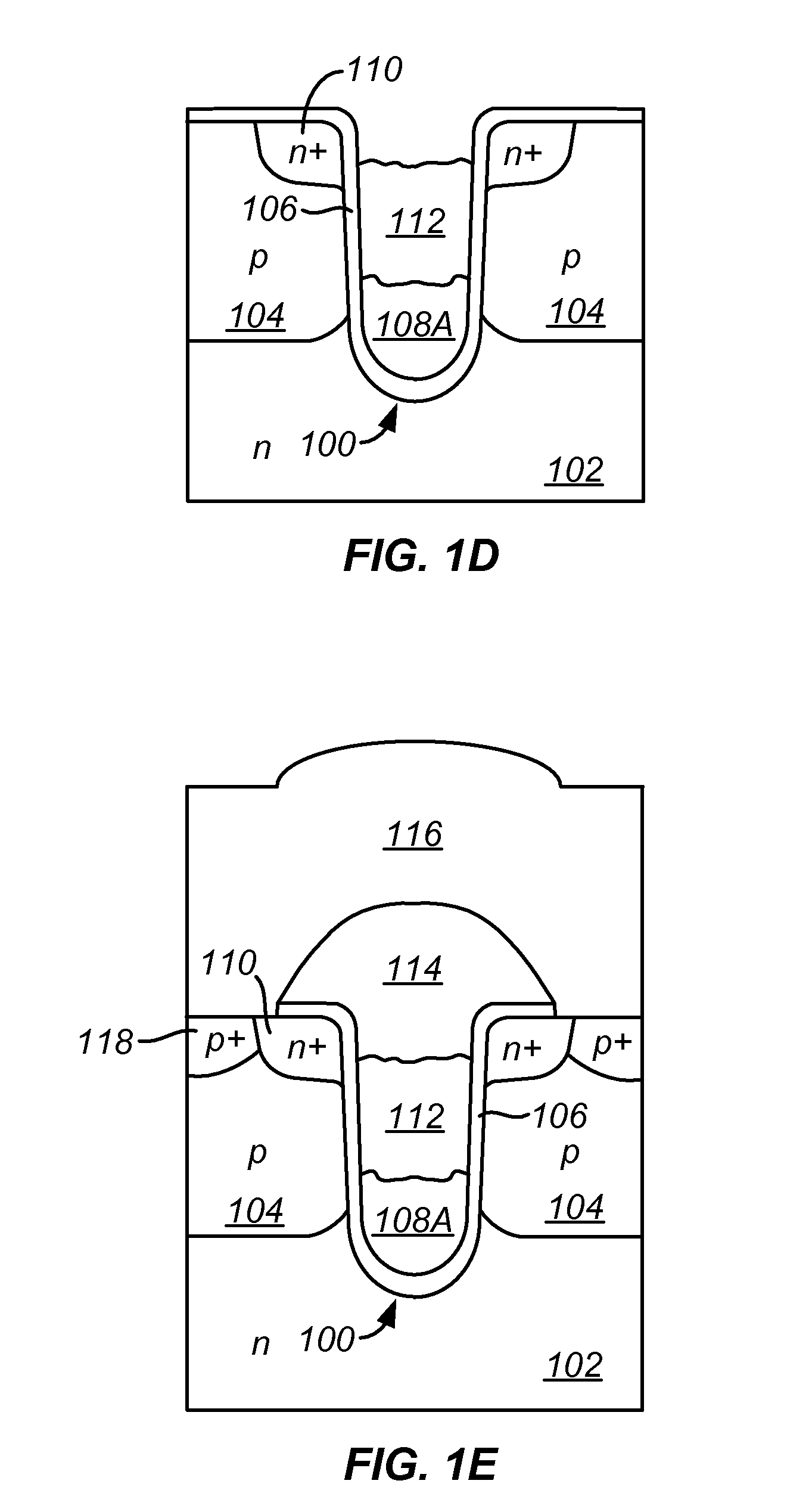
[0031]FIGS. 1A-1E show simplified cross section views at various stages of a manufacturing process for forming a trench gate MOSFET in accordance with an exemplary embodiment of the invention. In FIG. 1A, p-type well region 104, trench 100, and gate dielectric 106 lining the trench sidewalls and bottom are formed using conventional techniques. In FIG. 1B, a conductive layer 108 is formed filling trench 100 and extending over mesa surfaces. In FIG. 1C, conductive layer 108 is recessed to form seed layer 108A in trench 100.

[0032]Conductive materials with appropriate work function based on process integration and device requirement may be selecte...


PUM


Abstract

A trench gate field effect transistor is formed as follows. A trench is formed in a semiconductor region, followed by a dielectric layer lining sidewalls and bottom of the trench and extending over mesa regions adjacent the trench. A conductive seed layer is formed in a bottom portion of the trench over the dielectric layer. A low resistance material is grown over the conductive seed layer, wherein the low resistance material is selective to the conductive seed layer.

Description

CROSS-REFERENCE TO RELATED APPLICATIONS[0001]This application claims the benefit of U.S. Provisional Application No. 60 / 772,315, filed Feb. 10, 2006, and is also related to the commonly assigned U.S. application Ser. No. 11 / 026,276, filed Dec. 29, 2004. Both disclosures are incorporated herein by reference in their entirety for all purposes.BACKGROUND OF THE INVENTION[0002]Fast switching power transistors are needed to achieve voltage conversion at a minimum power loss. Low gate impedance is critical to achieving fast switching speeds and other performance parameters in such power devices as MOSFETs. However, as the devices are scaled down, the gate line-width gets narrower and the sheet resistance contribution to the equivalent series resistance (ESR) increases, adversely affecting the switching speed.[0003]Conventionally, the gate dopant concentration is increased to minimize the gate resistance. However, current doping concentrations are at saturation levels and any higher levels...

Claims


Application Information

Patent Timeline
Patent Type & Authority Applications(United States)
IPC IPC(8): H01L21/336H01L21/3205
CPCH01L29/42368H01L29/4925H01L29/4933H01L29/66734H01L29/4958H01L29/4966H01L29/513H01L29/4941
Inventor SREEKANTHAM, SREEVATSAHO, IHSIUSESSION, FREDNAYLOR, JAMES KENT
Owner SEMICON COMPONENTS IND LLC
Why Eureka
Try Eureka