Method of manufacturing semiconductor substrate and method of evaluating quality of semiconductor substrate

a technology of semiconductor substrate and manufacturing method, which is applied in the direction of semiconductor/solid-state device testing/measurement, lapping machines, instruments, etc., can solve the problems of contaminating the interior of the finished product substrate, and it is impossible to completely eliminate metal ions in the manufacturing of slurry, so as to reduce metal contamination

Active Publication Date: 2007-08-23
SUMCO CORP
View PDF4 Cites 8 Cited by
  • Summary
  • Abstract
  • Description
  • Claims
  • Application Information

AI Technical Summary

Benefits of technology

[0008] A feature of the present invention provides for a semiconductor substrate with reduced metal contamination.

Problems solved by technology

These metal ions diffuse into the interior of the wafer during the mirror polishing step, contaminating the interior of the finished product substrate.
However, in practice, it is impossible to completely eliminate metal ions in the manufacturing of a slurry.

Method used


Image

  • Method of manufacturing semiconductor substrate and method of evaluating quality of semiconductor substrate
  • Method of manufacturing semiconductor substrate and method of evaluating quality of semiconductor substrate
  • Method of manufacturing semiconductor substrate and method of evaluating quality of semiconductor substrate

Examples


example 1

[0060] Four eight-inch sliced silicon wafers were mirror polished with a slurry. Different slurries were employed for each wafer. Table 1 shows the results of measurement of the Cu, Ni, and Fe contents of each slurry by the atomic absorption method. The metal ions in slurry 1 were reduced by the addition of ethylenediaminetetraacetic acid.

TABLE 1Cu (ppb)Ni (ppb)Fe (ppb)Slurry 110101,000Slurry 2101001,000Slurry 3100101,000Slurry 410108,000

[0061] The silicon wafer subjected to mirror polishing with slurry 1 was denoted as sample 1, the silicon wafer subjected to mirror polishing with slurry 2 was denoted as sample 2, the silicon wafer subjected to mirror polishing with slurry 3 was denoted as sample 3, and the silicon wafer subjected to mirror polishing with slurry 4 was denoted as sample 4.

[0062] Table 2 shows the results obtained when each of the samples was inspected for particles with a foreign matter inspection device. In ordinary particle inspection, with respect to an eight-...

example 2

[0063] All of the samples prepared in Example 1 were inspected for metal contamination by the following method.

[0064] First, SC-1 cleaning was continuously conducted five times with a cleaning solution (NH4OH:H2O2:H2O=1:1:5) employed in SC-1 cleaning.

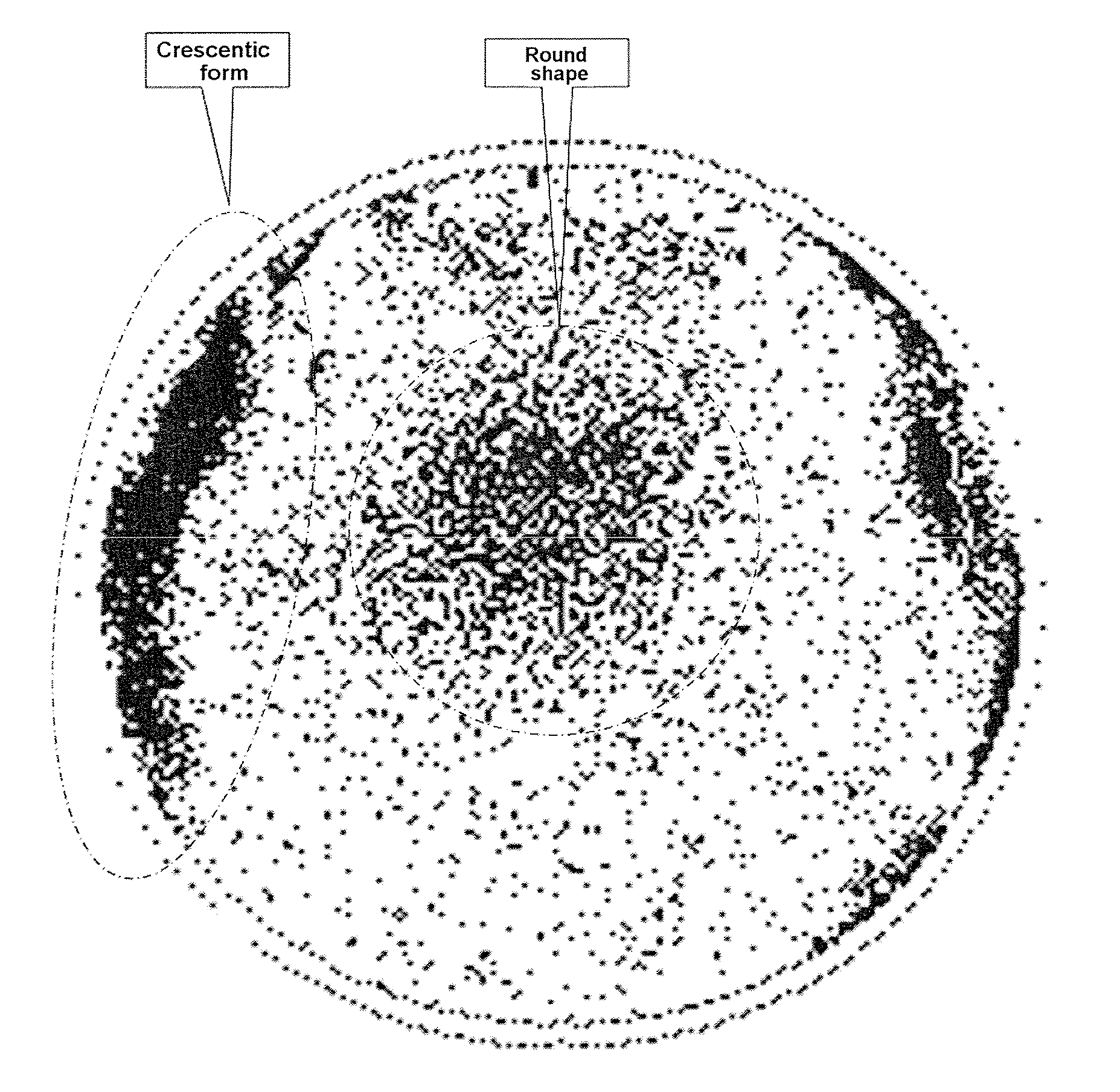
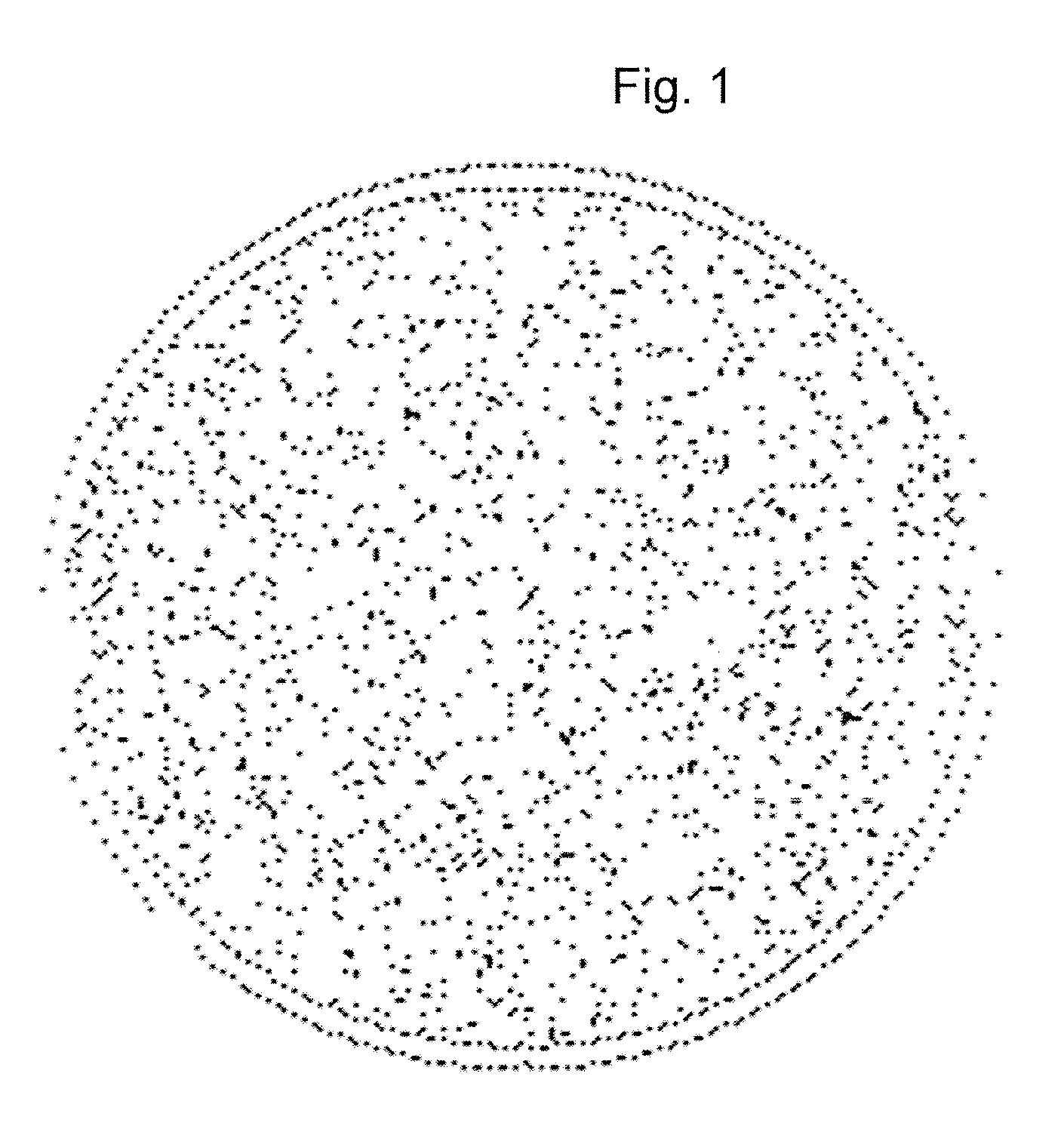
[0065] Next, the total number and the distribution pattern of bright points for each sample were measured with a foreign matter inspection device. The results are given in Table 3 and FIGS. 1 to 4. Table 3 shows the total number of bright points in each sample. FIGS. 1 to 4 show the distribution patterns of bright points in each sample. Taking into account the passing standard in particle inspection, samples with a total number of bright points not exceeding 3,000 were determined as a nondefective product.

TABLE 3Total number of bright pointsSample 11722Sample 24415Sample 3Equal to or greater than 30,000Sample 4Equal to or greater than 30,000

[0066] As indicated in Table 3, even among samples that passed the particle inspection, a met...

example 3

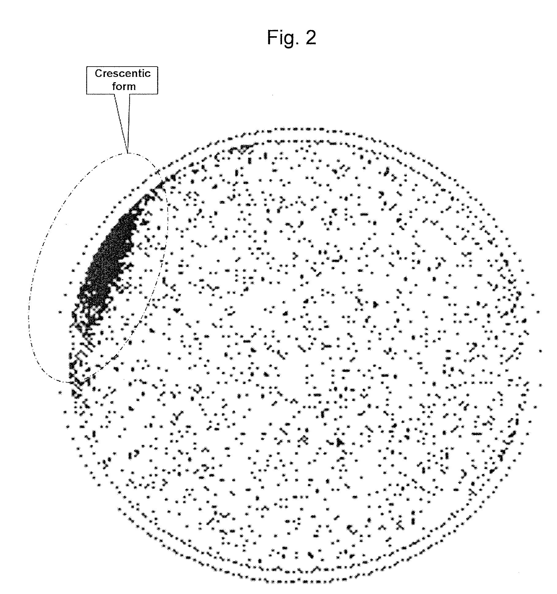
[0071] The surfaces of silicon wafers following mirror polishing were etched by being continuously SC-1 cleaned three times with a cleaning solution (NH4OH:H2O2:H2O=1:1:5) employed in SC-1 cleaning. A foreign matter inspection device was employed to detect bright points on the surfaces thereof; the results are given in FIG. 5. As indicated in FIG. 5, an abnormal portion (the “X” portion in FIG. 5) in which bright points were densely packed was observed in the peripheral portion in a map of bright points observed by the foreign matter inspection device. Then, this peculiar pattern was observed by scanning electron microscopy (SEM). The results are given in FIG. 6.

[0072] In the results of SEM observation as shown in FIG. 6, the abnormal portion was found to be a collection of pits. Observation at greater magnification revealed each pit to have a orientation. On this basis, the pits were presumed to have been caused by Cu.


PUM


Abstract

The method of manufacturing a semiconductor substrate including mirror polishing a silicon wafer surface, wherein the mirror polishing is conducted using a slurry having a Cu content of approximately equal to or less than 10 ppb, a Ni content of approximately equal to or less than 10 ppb, and an Fe content of approximately equal to or less than 1,000 ppb. The method of evaluating a quality of a semiconductor substrate including etching the surface of the semiconductor substrate by SC-1 cleaning and/or a HF cleaning, detecting bright points on the surface of the etched substrate with a foreign matter inspection device, and evaluating the quality of the semiconductor substrate based on the bright points detected on the surface of the substrate.

Description

CROSS-REFERENCE TO RELATED APPLICATIONS [0001] This application claims benefit of priority under 35 USC 119 to Japanese Patent Application No. 2005-345403 filed on Nov. 30, 2005, which is expressly incorporated herein by reference in its entirety. BACKGROUND OF THE INVENTION [0002] 1. Field of the Invention [0003] The present invention relates to a method of manufacturing a semiconductor substrate of reduced metal contamination and to a method of evaluating contamination and defects in a substrate. DISCUSSION OF THE BACKGROUND [0004] Generally, a semiconductor substrate serving as the base of a semiconductor part is manufactured by slicing to prescribed thickness a silicon single crystal ingot to fabricate a silicon wafer and then polishing one or both surfaces of the silicon wafer to a mirror finished surface with a mirror polishing device (for example, see Japanese Unexamined Patent Publication (KOKAI) No. 2001-102332, which is expressly incorporated herein by reference in its ent...

Claims


Application Information

Patent Timeline
Patent Type & Authority Applications(United States)
IPC IPC(8): H01L21/306B24B37/00H01L21/304H01L21/66
CPCG01N1/32Y10T436/104998H01L21/02024
Inventor MIYAZAKI, MORIMASAKITAMURA, TAKAFUMIIWASHITA, TETSUROOHIRA, MIHOKO
Owner SUMCO CORP
Why Eureka
Try Eureka