Impedance matching via structure for high-speed printed circuit boards and method of determining same

a technology of printed circuit boards and via structures, which is applied in the direction of printed circuit components, printed circuit adaptations, printed circuit manufacturing, etc., can solve the problems of impedance mismatch at the via transition, physical size of the circuit continues to shrink, and the impedance mismatch poses a serious problem, so as to improve the signal transition, reduce radiation loss, and reduce the effect of signal reflection

Inactive Publication Date: 2007-08-23
MICRON TECH INC
View PDF10 Cites 22 Cited by
  • Summary
  • Abstract
  • Description
  • Claims
  • Application Information

AI Technical Summary

Benefits of technology

[0009] An exemplary implementation of the present invention includes an impedance matching conductive via structure that is effectively constructed by selecting an outer conductor and an inner conductor (a via cylinder) diameter through analytical calculation or numerical simulation, such that impedance of the conductive via structure is matched to the impedance of the conductive signal traces of a printed circuit board. The conductive via structure comprises a conductive barrel that either connects to multiple ground planes or to multiple power planes and serves as the outer conductor for a coaxial structure. The conductive via structure also provides a current return path and a matched impedance path of via transition, thus greatly improving the signal transition and reducing signal reflection due to via discontinuity. Moreover, the conductive barrel of the conductive via structure also reduces radiation loss through a parallel plane structure and suppresses coupling between neighboring vias as energy escaping through the conductive barrel and radiating to other vias is minimized.

Problems solved by technology

Due to the intrinsic geometrical difference between via and its connected traces, there exists impedance mismatch at a via transition.
As circuit switching speed dramatically increases into the multi-Gbps range, and the physical size of the circuit continues to shrink, this via impedance mismatch poses a serious problem.
This impedance mismatch gets worse as signal transition speeds dramatically increase into the multi-Gbps range.
As the frequency increases, the electrical length of a via impedance mismatching section becomes longer in relation to the signal and poses a more serious problem than at a low frequency range.
Also, as the physical size of the circuit becomes more compact the via diameter shrinks as well, and this shrinkage in size increases the inductance of the via structure, which, in turn, increases the impedance mismatch of the via structure.
Such impedance mismatch degrades signal integrity and consumes operating voltage margin.
Such signal degradation inevitably lowers the voltage margin for high-speed applications.

Method used


Image

  • Impedance matching via structure for high-speed printed circuit boards and method of determining same
  • Impedance matching via structure for high-speed printed circuit boards and method of determining same
  • Impedance matching via structure for high-speed printed circuit boards and method of determining same

Examples


Embodiment Construction

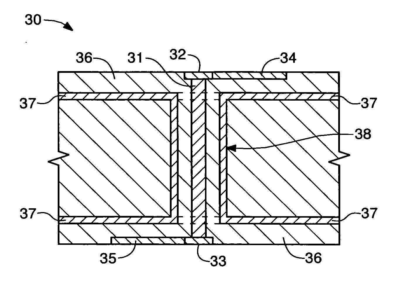
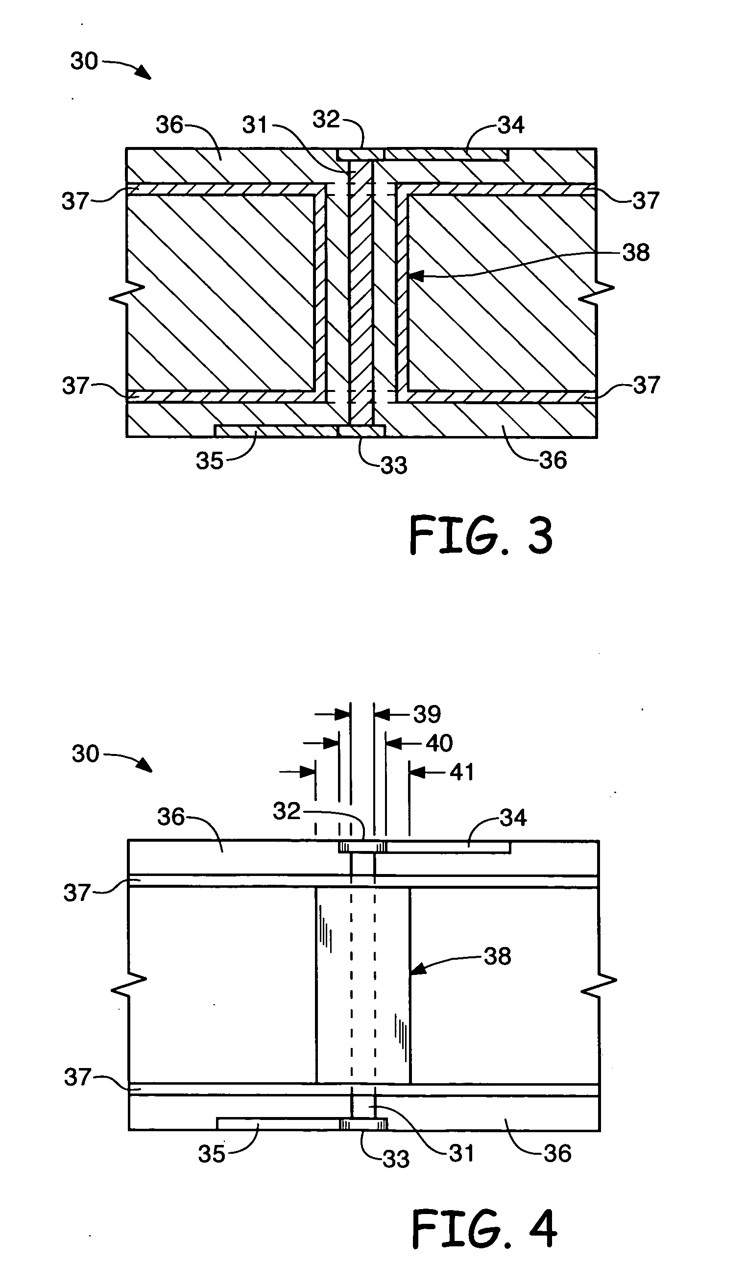
[0018] An exemplary implementation of the present invention is directed to a printed circuit board via structure and a design process for forming same, as depicted in FIGS. 3 and 4.

[0019] Referring to FIG. 3, the cross sectional view of PCB member 30 shows a conductive cylindrical barrel 38 extending around and in electrical isolation from via cylinder 31 which forms an impedance matching PCB via structure. Top conductive via pad 32 and bottom conductive via pad 33 connect to the top and bottom ends of via cylinder 31, respectively. Top and bottom conductive signal interconnect traces 34 and 35 connect to top conductive via pad 32 and bottom conductive via pad 33, respectively. The conductive cylindrical barrel 38 is added around the via cylinder structure 31.

[0020] Referring to both in FIG. 3 and FIG. 4, conductive barrel 38 connects to both ground planes 37 (or to other power planes depending on the PCB design) and serves as the outer conductor which forms a coaxial structure in...


PUM


Abstract

An impedance matching conductive via structure that is effectively constructed by selecting an outer conductor and an inner conductor diameter through analytical calculation or numerical simulation, such that impedance of the conductive via structure is matched to the impedance of the conductive signal traces of a printed circuit board. The conductive via structure comprises a conductive barrel that either connects to multiple ground planes or to multiple powers planes and serves as the outer conductor for a coaxial structure that provides a current return path and a matched impedance path of via transition, thus improving the signal transition and reducing signal reflection due to via discontinuity. Moreover, the conductive barrel of the conductive via structure also reduces radiation loss through a parallel plane structure and suppresses coupling between neighboring vias as the energy escaping through the conductive barrel and radiating to other vias is minimized.

Description

FIELD OF THE INVENTION [0001] This invention relates to a semiconductor interconnect structure and the design method thereof and, more particularly, to a printed circuit board (PCB) interconnect structure and the design method thereof. BACKGROUND OF THE INVENTION [0002] For high-speed digital PCB design, through-hole vias (openings) are used extensively to connect signal traces on different layers. Due to the intrinsic geometrical difference between via and its connected traces, there exists impedance mismatch at a via transition. As circuit switching speed dramatically increases into the multi-Gbps range, and the physical size of the circuit continues to shrink, this via impedance mismatch poses a serious problem. [0003] In a multi-layer PCB structure, vias are used extensively to facilitate routing of signal traces from one signal layer to another. As mentioned, due to the intrinsic geometrical difference between a via and signal traces (typically, one is in the form of a cylindri...

Claims


Application Information

Patent Timeline
Patent Type & Authority Applications(United States)
IPC IPC(8): H05K1/11H01R12/04
CPCH05K1/0222H05K1/0251H05K2201/09809H05K3/429H05K1/115
Inventor CHEN, HOUFEIZHAO, SHIYOU
Owner MICRON TECH INC
Why Eureka
Try Eureka