High efficiency LEDs with tunnel junctions

a technology of leds and tunnel junctions, applied in the direction of semiconductor devices, basic electric elements, electrical apparatus, etc., can solve the problems of poor electrical conductivity, more resistive current flow, and non-uniform current injection into the active layer, and achieve high efficiency

Active Publication Date: 2007-08-23
CREELED INC
View PDF10 Cites 129 Cited by
  • Summary
  • Abstract
  • Description
  • Claims
  • Application Information

AI Technical Summary

Problems solved by technology

One disadvantage of wide band gap p-type confinement layers is that they are more resistive to current flow (i.e. poor electrical conductivity) compared to n-type wide band gap layers.
This results in non-uniform current injection into the active layer and reduced efficiency of the overall device.
While this does result in effective current spreading, the contact can absorb much of the light emitting from active layer through the p-type layer, reducing the overall efficiency of the device.
This robust metal layer, however, will be opaque to the light generated by the active region.
Some metals capable of forming ohmic contacts to wide band gap p-type layers do not effectively adhere to the surface of the p-type layer.
This poor adherence can require the deposition of a two-layer semi-transparent window for the p-type metal contact.
Another characteristic of p-type wide band gap layers is that they are more fragile than n-type wide band gap layers, which can lead to complications in processing wide band gap photonic devices.
This is especially difficult in photonic devices where many processing takes place after the deposition of the p-type layers.
One difficulty with this approach is tunnel diodes in wide band gap materials tend to be inefficient and highly resistive to current flow.
The band gap of wide band gap materials tends to significantly degrade the performance of the tunnel junction, while the saturation level of dopants in wide band gap materials is such that even degenerate doping does not reduce the resistance to tunneling encountered by the wide band gap material sufficient to make the device efficient.
A tunnel junction contact to a p-type confinement layer in a wide band gap photonic device with a low tunneling resistance is difficult to form, because of the large band gap and doping limitations that prevent the formation of very thin tunnel widths.

Method used


Image

  • High efficiency LEDs with tunnel junctions
  • High efficiency LEDs with tunnel junctions
  • High efficiency LEDs with tunnel junctions

Examples


Embodiment Construction

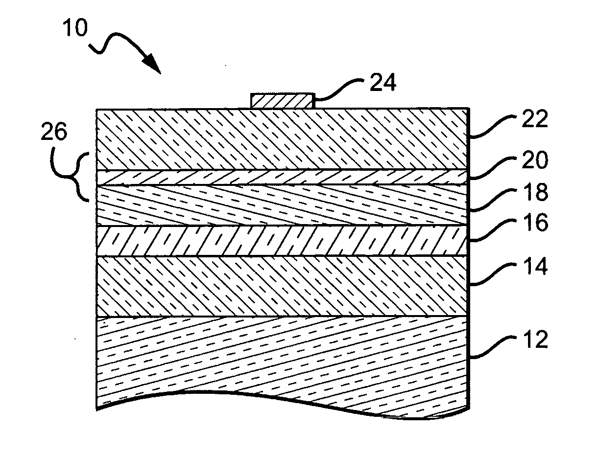
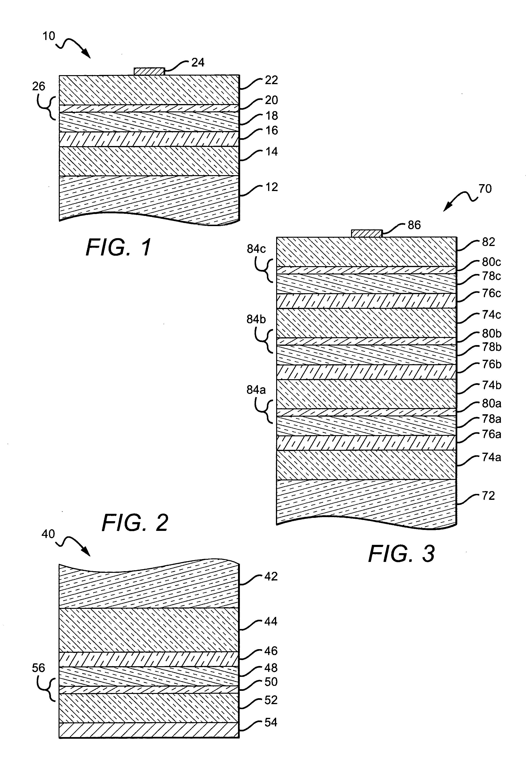
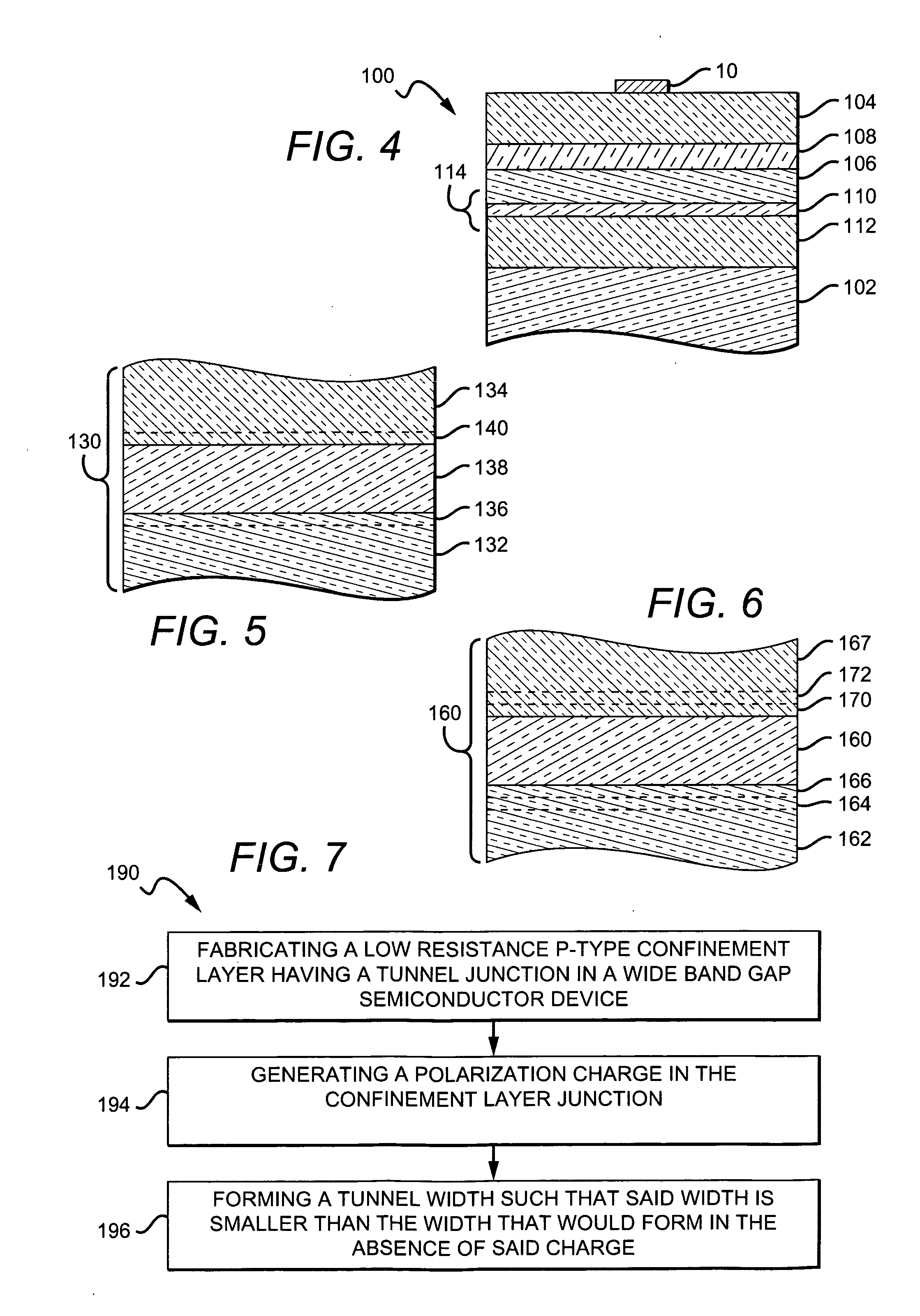
[0027] The following describes devices having a construction with crystal layers grown normal to a polar direction of the crystal. In one embodiment, device layers are presumed to have the Wurtzite crystal structure with layers comprising gallium nitride (GaN), indium gallium nitride (InxGayN), and aluminum gallium nitride (AlxGayN) where 0.3≦x≦1.0 and x+y=1.0. Except where noted, the top surface of the crystal has (0001) orientation with Periodic Table group III polarity.

[0028] The devices disclosed comprise semiconductor materials typically prepared by epitaxial growth methods. Epitaxial growth methods grow uniform two-dimensional surfaces where variations in compositions and doping may be made in a third dimension as growth proceeds over time. Typically, these structures are grown by molecular beam epitaxy (MBE) or metal organic chemical vapor deposition (MOCVD). However, other equally useful methods of epitaxial growth may be used to achieve these ends.

[0029] Some of the follo...


PUM


Abstract

An LED made from a wide band gap semiconductor material and having a low resistance p-type confinement layer with a tunnel junction in a wide band gap semiconductor device is disclosed. A dissimilar material is placed at the tunnel junction where the material generates a natural dipole. This natural dipole is used to form a junction having a tunnel width that is smaller than such a width would be without the dissimilar material. A low resistance p-type confinement layer having a tunnel junction in a wide band gap semiconductor device may be fabricated by generating a polarization charge in the junction of the confinement layer, and forming a tunnel width in the junction that is smaller than the width would be without the polarization charge. Tunneling through the tunnel junction in the confinement layer may be enhanced by the addition of impurities within the junction. These impurities may form band gap states in the junction.

Description

BACKGROUND OF THE INVENTION [0001] 1. Field of the Invention [0002] The present invention relates to semiconductors devices formed from wide band gap materials, and in particular wide band gap light emitting semiconductor devices utilizing tunnel junctions to increase device light emitting efficiency and to increase the device surface robustness to post growth processing steps. [0003] 2. Description of the Related Art [0004] Photonic devices such as light emitting diodes (LED's) and quantum well lasers having a single quantum well (SQW) or multiple quantum wells (MQW) have been fabricated from wide band gap materials. These wide band gap materials include but are not limited to gallium nitride (GaN), indium nitride (InN), aluminum nitride (AlN) and combinations thereof. Photonic semiconductor devices have been described in the Physics of Semiconductors, 2nd Ed., SZE, Wiley Interscience, 1981 Chapter 12, pp. 681-742. Wide band gap materials are described in Solid State Electronic Dev...

Claims


Application Information

Patent Timeline
Patent Type & Authority Applications(United States)
IPC IPC(8): H01L33/00H01L33/04H01L33/08H01L33/32
CPCH01L33/0016H01L33/32H01L33/08H01L33/04
Inventor IBBETSON, JAMES P.KELLER, BERND P.MISHRA, UMESH K.
Owner CREELED INC
Why Eureka
Try Eureka