Light emitting device having vertical structure, package thereof and method for manufacturing the same
a technology of light emitting devices and vertical structures, which is applied in the direction of semiconductor devices, basic electric elements, electrical appliances, etc., can solve the problems of high production costs, low efficiency, and the inability of green leds fabricated using this material to produce pure green light, so as to reduce the number of processes and processing time, the effect of preventing damage to a semiconductor thin film
- Summary
- Abstract
- Description
- Claims
- Application Information
AI Technical Summary
Benefits of technology
Problems solved by technology
Method used
Image

Examples
first embodiment
[0075] Hereinafter, a first embodiment of the present invention will be described with reference to the accompanying drawings.
[0076] First, a method for manufacturing individual semiconductor light emitting device chips will be described.
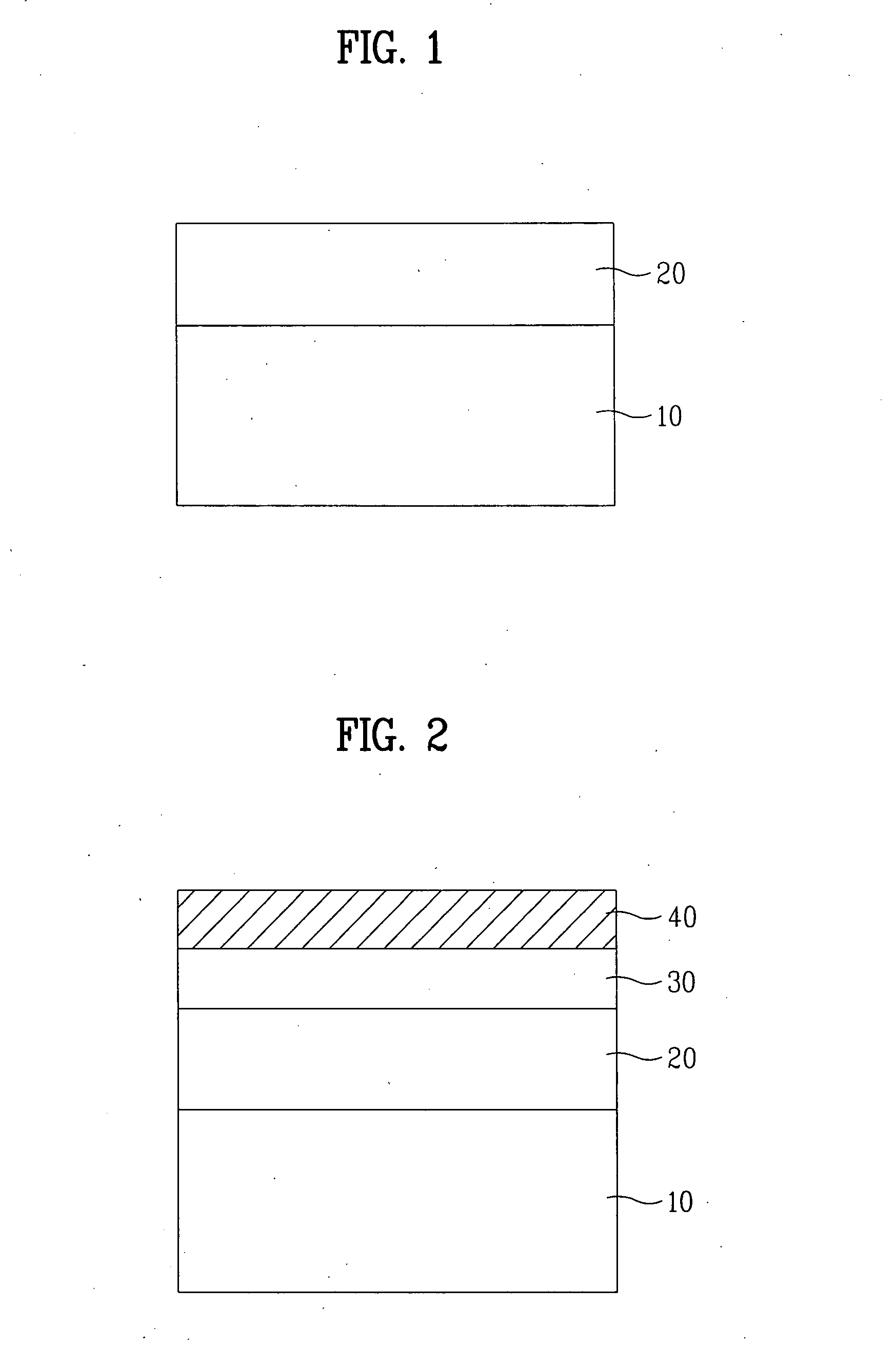
[0077] As shown in FIG. 1, in order to manufacture a light emitting device chip according to this embodiment, a semiconductor layer 20 having a multilayer structure is formed over a sapphire substrate 10, using a thin film growing method such as a hydride vapor phase epitaxy (HVPE) or a metal organic chemical vapor deposition (MOCVD) method. The HVPE method is advantageous in that it is possible to grow a thin film having a low impurity concentration, namely, a high purity, at a high growth rate of 50 to 100 μm per hour.
[0078] The growth of the semiconductor layer 20, which has a multilayer structure, can be achieved by first forming an n type GaN semiconductor layer over the substrate 10, forming an active layer over the n type GaN semiconductor...
second embodiment
[0132] Hereinafter, a second embodiment of the present invention will be described with reference to FIGS. 20 to 30. No description may be given of the processes of the second embodiment identical to those of the first embodiment.
[0133] First, a method for manufacturing individual semiconductor light emitting device chips will be described.
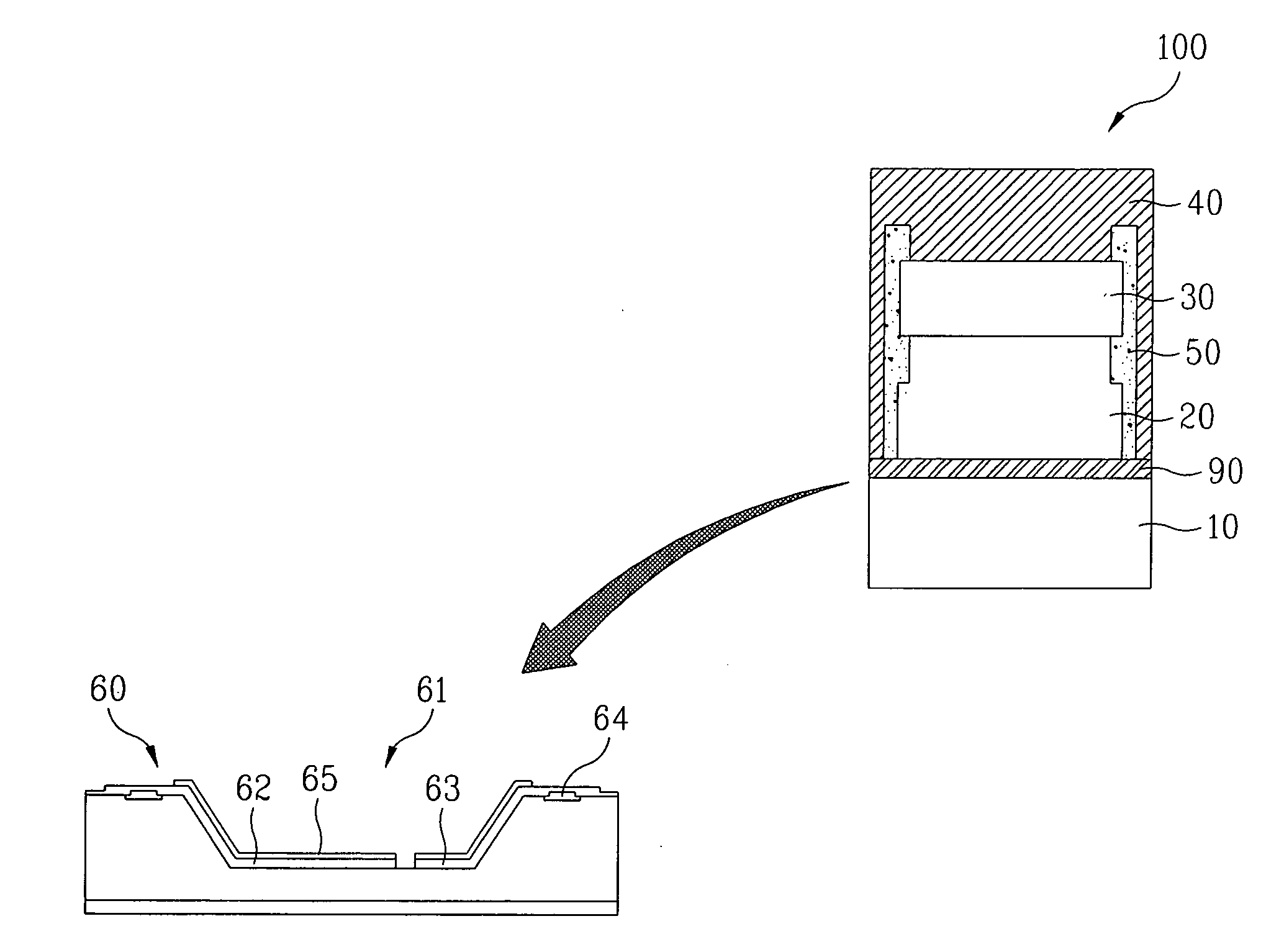
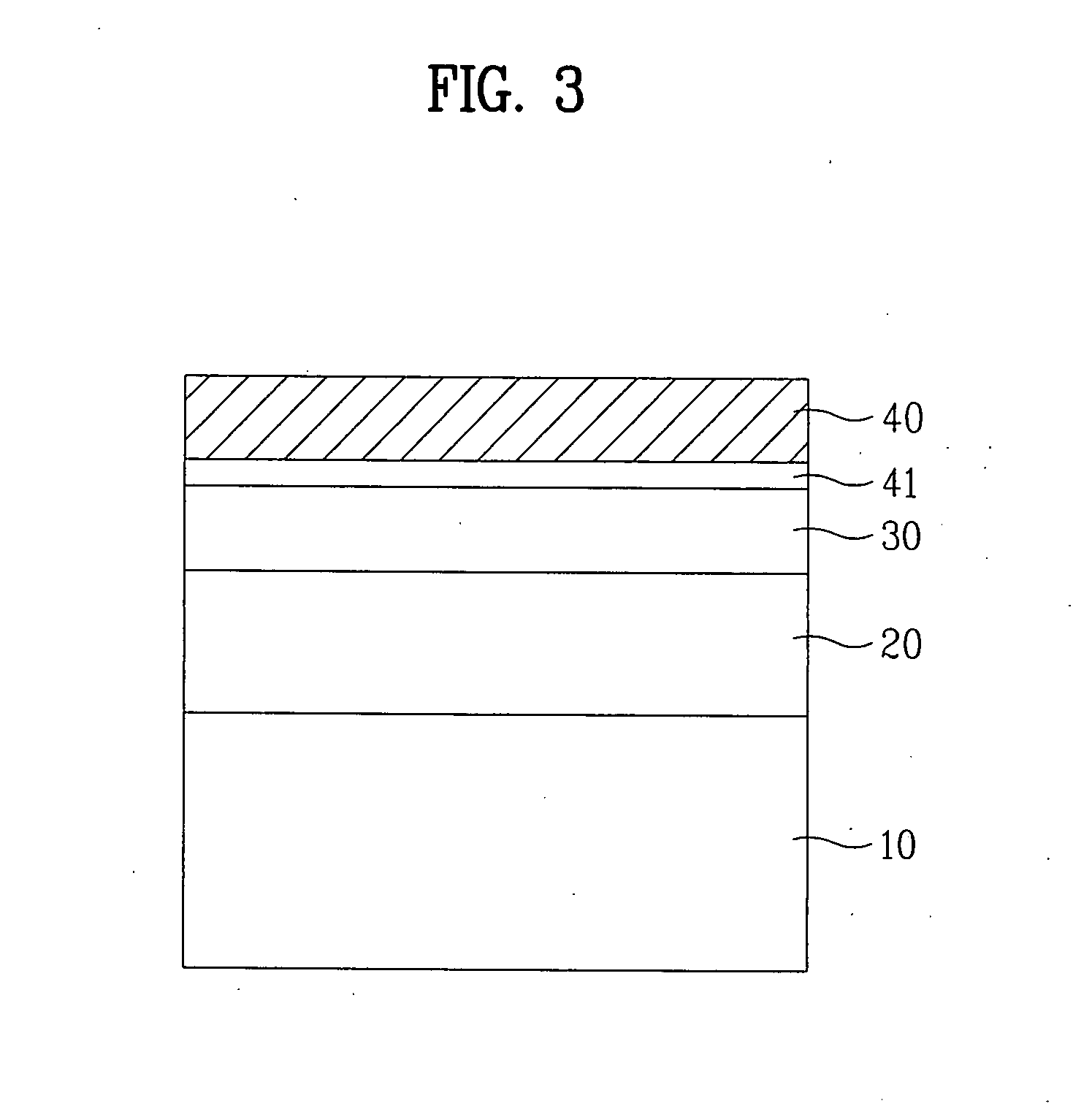
[0134] As shown in FIG. 20, in order to manufacture a light emitting device chip according to this embodiment, a semiconductor layer 20 having a multilayer structure is formed over a sapphire substrate 10, using a thin film growing method such as a hydride vapor phase epitaxy (HVPE) or a metal organic chemical vapor deposition (MOCVD) method, after formation of a metal buffer layer 90 over the sapphire substrate 10.
[0135] The growth of the semiconductor layer 20, which has a multilayer structure, can be achieved by first forming an n type GaN semiconductor layer over the substrate 10, forming an active layer over the n type GaN semiconductor la...
PUM
 Abstract
Description
Claims
Application Information
 - Generate Ideas
- Intellectual Property
- Life Sciences
- Materials
- Tech Scout
- Unparalleled Data Quality
- Higher Quality Content
- 60% Fewer Hallucinations
Browse by: Latest US Patents, China's latest patents, Technical Efficacy Thesaurus, Application Domain, Technology Topic, Popular Technical Reports.
© 2025 PatSnap. All rights reserved.Legal|Privacy policy|Modern Slavery Act Transparency Statement|Sitemap|About US| Contact US: help@patsnap.com