Electronic circuit, a semiconductor device and a mounting substrate

a technology of semiconductor devices and mounting substrates, applied in the field of electronic circuits, can solve the problems of strict restriction of the timing margin of data signals (dq) which correspond to data strobe signals (dqs) outputted from respective memory chips, and achieve the effect of enhancing conversion accuracy and preventing switching noises of switches

Inactive Publication Date: 2007-08-23
RENESAS ELECTRONICS CORP
View PDF5 Cites 54 Cited by
  • Summary
  • Abstract
  • Description
  • Claims
  • Application Information

AI Technical Summary

Benefits of technology

[0052] According to another aspect of the present invention, in the semiconductor device of the present invention, the semiconductor chip is mounted on the package substrate, the semiconductor chip includes a DAC (334), and the package substrate includes a first conductive layer which is used for connection with pad electrodes of the semiconductor chip, a second conductive layer which is used as the ground plane, a third conductive layer which is used as the power source plane, and a fourth conductive layer which is used for connection with the mounting substrate. The above-mentioned DAC includes a circuit which adds a constant current from the constant current source circuit (390) to an output node using a switch (391). The semiconductor chip (31) includes a first analog power source terminal (VCCA) and a first analog ground terminal (VSSA) for the constant current source circuit and a second analog power source terminal (VCCA1) and a ...

Problems solved by technology

However, in the DDR-SDRAM interface specification, to realize the high-speed property of the interface, not only the equal-length property of the clock lines is to be s...

Method used


Image

  • Electronic circuit, a semiconductor device and a mounting substrate
  • Electronic circuit, a semiconductor device and a mounting substrate
  • Electronic circuit, a semiconductor device and a mounting substrate

Examples


Embodiment Construction

[0095]>

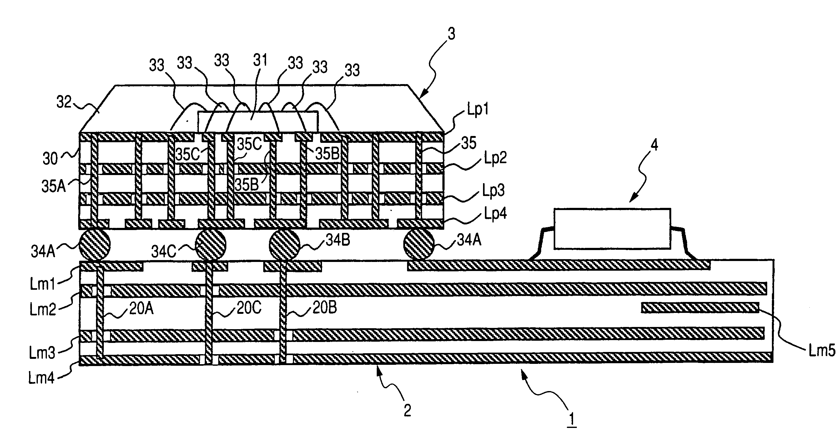
[0096]FIG. 1 shows one example of an electronic circuit according to the present invention. An electronic circuit 1 shown in the FIG. 1 includes a data processor 3 which constitutes a first semiconductor device and a SDRAM 4 which constitutes a second semiconductor device on a mounting substrate 2. Although not particularly shown in the drawing, a plurality of SDRAMs 4 is mounted on the mounting substrate 2.

[0097] The data processor 3 includes a package substrate 30 which has the BGA package structure, for example, and a processor chip 31 which is mounted on the package substrate 30, wherein a surface of the data processor 3 is protected by a sealing resin 32. Although not particularly limited, the SDRAM 4 is constituted by sealing a SDRAM chip in a flat package such as a SOP (Small Outline Package). The processor chip 31 and the SDRAM chip not shown in the drawing are, although not particularly limited, formed on one semiconductor substrate made of mono-crystalline silicon ...


PUM


Abstract

An electronic circuit includes a first semiconductor device (4) and a second semiconductor device (3) on a mounting substrate. The mounting substrate includes a plurality of mounting substrate lines (201 to 204) which are connected in common with external terminals of a plurality of bits of the first semiconductor device and external terminals of a plurality of bits of the second semiconductor device for every bit. The mounting substrate lines have lengths thereof from the external terminals of the first semiconductor device to the external terminals of the second semiconductor device made unequal for respective bits. Assembling lines (361 to 364) which reach connecting electrodes of a semiconductor chip from the external terminals of the second semiconductor device have made lengths thereof unequal for respective bits. Here, the unequal lengths of the mounting substrate lines have a relationship which offsets the unequal lengths of the assembling lines. According to such a constitution, it is unnecessary to set lengths between the external terminals of the second semiconductor device and the connecting electrodes of the semiconductor chip equal.

Description

TECHNICAL FIELD [0001] The present invention relates to an electronic circuit in which a semiconductor device is mounted on a mounting substrate, a semiconductor device and a mounting substrate, and, for example, to a technique which is effectively applicable to a circuit module which mounts a data processor and an SDRAM (Synchronous Dynamic Random Access Memory), particularly DDR (Double Data Rate)-SDRAM (JEDEC STANDARD: JESD79) on a mounting substrate having the multi-layered wiring structure. BACKGROUND ART [0002] As a document which describes a circuit module which mounts a data processor and an SDRAM on a mounting substrate, there has been known Japanese Patent Laid-open 2001-177046. According to this document, the data processor having the BGA package structure is arranged at the center, the SDRAM is arranged around the data processor, and data terminals for the SDRAM are arranged at a center portion of a side of the BGA (Ball Grid Array) package. Output terminals of clocks, a...

Claims


Application Information

Patent Timeline
IPC IPC(8): H01L23/12G06F1/18G06F12/00G06F13/16H01L23/498H01L23/552H01L25/10H01L25/18H05K1/00H05K1/02H05K1/11H05K1/18
CPCH01L23/49838H01L23/552H01L2924/12041H01L2224/48227H01L2224/48235H01L2924/01057H01L2924/01078H01L2924/01079H01L2924/15173H01L2924/15311H01L2924/30107H01L2924/3011H01L2924/3025H05K1/0216H05K1/023H05K1/0246H05K1/0248H05K1/0298H05K1/112H05K1/181H05K2201/09227H05K2201/09236H05K2201/09263H05K2201/093H05K2201/10022H05K2201/10159H05K2201/10522H05K2201/10689H05K2201/10734H01L24/48H01L2924/01019H01L2924/01055H01L2924/00H01L24/49H01L2224/48091H01L2224/49171H01L2924/00014H01L2924/14H01L2924/181Y02P70/50H01L2924/00012H01L2224/45099H01L2224/45015H01L2924/207
Inventor SUWA, MOTOOMIYAKI, YOSHINORIHAYASHI, TORUSANO, RYOICHIMATSUI, SHIGEZUMINARUSE, TAKANOBUSATO, TAKASHISHIOTA, HISASHI
Owner RENESAS ELECTRONICS CORP
Why Eureka
Try Eureka